

The Computex trade show in Taipei, Taiwan is the traditional place where Intel has put out its Xeon E3 processors for diminutive and graphics-accelerated servers, and this week the chip maker is indeed rolling out a variant of this chip using its “Broadwell” cores. Intel is also completing the rollout of Xeon parts based on the prior “Haswell” cores with the delivery of a Xeon E5 aimed specifically at dense four-socket servers.
The Xeon E5-4600 v3 processor based on the Haswell cores slides right in between the Xeon E7 v3 processors that Intel launched in May for machines with four or more sockets and the Xeon E5-2600 v3 chips that the company put into the field back in September 2014 for machines with two sockets. As with the two prior generations of the E5-4600 series of processors, the Haswell version uses the pair of QuickPath Interconnect (QPI) point-to-point links to cross-connect up to four sockets together. On the high-end Xeon E7 processors, the chips have three QPI ports, which means four-sockets can be directly linked to each other and that on an eight-socket machine, no socket is more than two hops away. With the E5 chips and their pair of QPI ports, two sockets have a pair of links sharing information across the sockets, which provides excellent NUMA scaling; with four sockets, the pair of QPI links on each chip can hook one chip to its two adjacent partners, but the fourth chip is two hops away. The NUMA scaling takes a hit just as it does a bit on an eight-way machine with the Xeon E7s.
Generally speaking, the Xeon E5-4600s are aimed at workloads that do not require the large memory footprint of the Xeon E7, which allows for up to 24 memory slots per socket compared to the 12 memory slots in the Xeon E5s. Think server virtualization and database acceleration, but not at an extreme memory capacity that is possible with the Xeon E7s. The upshot is that a four-way Xeon E7-4800 v3 chip with four sockets can support up to 6 TB of main memory across those sockets compared to a maximum of 3 TB across the four sockets in a system based on the Xeon E5-4600 v3 processors. Because the Xeon E7 has twice as many memory slots and uses an outboard memory buffer chip to be able to support such memory capacities, the typical four-socket Xeon E7 node is 4U or 5U tall, compared to the Xeon E5-4600 machines, which can be crammed into a 2U space. The Xeon E5-4600s generally cost a bit less, too, but not by all that much.
The important thing, as Hewlett-Packard explained when it retooled its ProLiant server lineup for the Xeon E5 and E7 processors recently, is that the E5-4600s allow for a higher ratio of compute to memory than the Xeon E7-4800s. (In 4U of space in a rack, you can get eight sockets and up to 6 TB of memory with the E5-4600 v3s, compared to four sockets and 6 TB of memory with the E7-4800 v3s.) HP tells The Next Platform that four-socket E7 boxes still outsell four-socket E5 machines, but both types are popular with memory-heavy workloads.
Like other Haswell generation processors, the Xeon E5-4600s support DDR4 main memory, which can yield up to 1.4X times the memory bandwidth as the prior “Ivy Bridge” Xeon E5-4600 processors; the DDR4 main memory runs a little cooler, too. The Haswell Xeon E5-4600s have up to 50 percent more cores and provide an average of around 49 percent more performance than their Ivy Bridge predecessors (a similar span to the two most recent generations of Xeon E5-2600 chips). The Haswell cores also support AVX2 vector instructions, which provide twice the floating point oomph of the Ivy Bridge cores. So, the Xeon E5-4600s would also make a reasonable fat node in an HPC cluster if the Xeon E5-2600s did not deliver enough memory at 1.5 TB per system. (The machines might even make a decent node for HANA in-memory clusters, but thus far SAP has certified only on Xeon E7 chips and Power8 chips.) The Haswell cores also support Intel’s QuickAssist Technology for offloading encryption from the cores to dedicated accelerators, which can boost encryption performance by a factor of 2X.
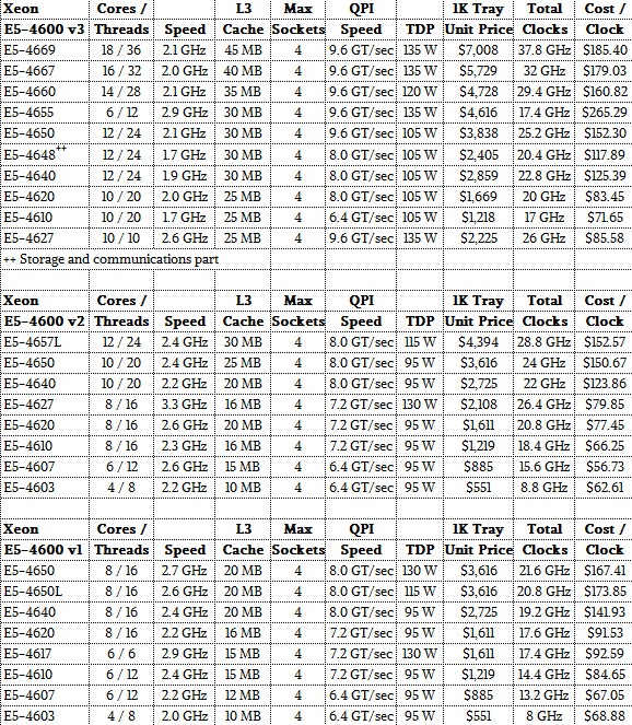
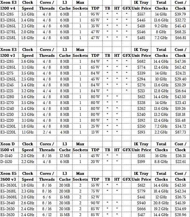
Some things to note about the Xeon E5-4600 v3 family. While the core counts, L3 cache sizes, and QPI speeds have gone up, the clock speeds on the cores have come down a smidgen on a SKU for SKU basis. The thermal design point (TDP) ratings for the v3 version of the chips includes the integrated voltage regulator, which the prior v2 and v1 chips did not have.
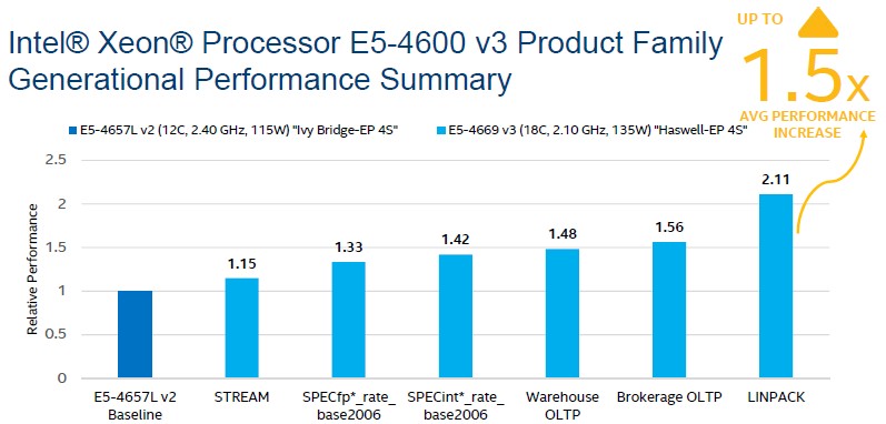
As we went to press, Intel did not have its usual suite of benchmark test results available across all SKUs, so we counted up the total clocks in each chip to get a rough sense of the relative performance and price/performance across these generations of processors. As you can see from the table above, the extra performance in the v3 parts is coming at a price. For instance, the top-bin Haswell E5-4669 v3 chip delivers around 31 percent more oomph than the E5-4657L v2 that was the top of the Ivy Bridge lineup in the 4600 series, but it costs 59 percent more at $7,008 per chip when bought in 1,000-unit trays. On like-for-like SKUs – or as close as we can get to them – the premium ranges from 7 percent to 49 percent – for the added cache, higher QPI speeds, more floating point math, and other differences between the generations. (Our oomph performance factors do not take into account tweaks in the cores that improved instructions per clock processed, which would close some of that gap but certainly not all of it.)
Intel has a special part called the E5-4648 v3 that is aimed at storage and communications workloads, but the exact nature of this chip was not discussed, but it has a larger L3 cache and faster QPI links than you would expect given its core count and clock speed; it also has a lower price relative to its features and the other Xeon E5-4600 v3 chips in the lineup and presumably supports Intel’s Rapid Storage Technology 12x feature, which adds RAID data protection and other tunings to boost storage performance.
The E5-4655 is also an interesting outlier in that it has only six cores active and is presumably, like other Xeon E7 chips in the Haswell line, aimed at database workloads where high clock speed improves certain kinds of performance and low core count means a drop in software licensing costs.
We will gin up some server configurations once they are available and see how Xeon E5-4600 systems stack up against Xeon E5-2600s and Xeon E7-4800s and E7-8800s.
From Microserver To Video Transcoding And Remote Workstations
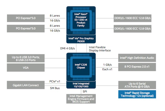
Intel spent a lot more time talking about the new Broadwell Xeon E3-1200 v4 processors at Computex than it did the Xeon E5-4600 v3s. These Xeon E3 chips are somewhat less relevant to a lot of enterprise workloads but are important in that they provide a hybrid compute platform that mixes Xeon CPUs with Intel’s Iris Pro Graphics P6300 GPUs. Intel has not been aggressive in trying to get companies to use these integrated GPUs in the Xeon E3 processors as general-purpose accelerators, and in fact with prior generations Intel sold variants of the Xeon E3 chips with the GPUs either not in the package or with the circuits turns off if they were on die.
In the wake of Intel’s pending $16.7 billion acquisition of field programmable gate array maker Altera, announced earlier this week, one can envision global replacing the GPU with an FPGA to come up with what a hybrid Xeon-Stratix compute unit might look like. Intel has said that it will offer such a hybrid in a single package at first, as it originally did with Xeon CPUs and Iris GPUs, and then move to a monolithic die, as it did with the Haswell variant of the Xeon E3s when they launched two years ago. (Yes, the Haswell rollout has taken two years in the datacenter. And it doesn’t look like it will take two years for the Broadwell Xeon rollout from E3 bottom to E7 top, either.)
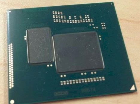
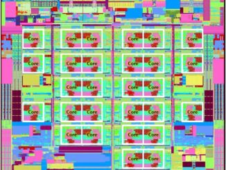
Aside from the integrated graphics and media streaming and transcoding offload that this enables, the Broadwell Xeon E3 v4 chip is interesting in that it is the first standard Intel part to include embedded DRAM cache memory. (The way Intel answered that question leads me to believe, on merely a hunch, that custom Xeon parts might already include eDRAM on the package. . . .) Specifically, as you can see in the package shot above, the chip on the left is a 128 MB chunk of eDRAM, which burns with less juice than regular DRAM and therefore can be used as a chip cache either in package or on die. And if Intel is like IBM, it will eventually move eDRAM onto the die as Moore’s Law enables more transistors on the die.
There were thirteen Xeon E3 v2 chips, but with the Broadwell E3s, Intel is cutting the SKUs back to five. (The two Xeon D processors, also based on the Broadwell cores and announced back in March mainly for hyperscale datacenters, are not variants of the Xeon E3s, but rather the Xeon E5s.) For all we know, there are custom parts that Intel is making that increases the total Broadwell Xeon E3 count, but I somehow doubt that. The Xeon D was about satisfying the needs of hyperscalers in two fell swoops, and presumably Facebook is first in line using them because it talked so much about it and dedicated its “Yosemite” microserver design to the chip.
Here’s a table comparing the v4 and v3 generations of the Xeon E3s to the Xeon Ds and the low-voltage variants of the Xeon E5 v3 chips:
There are a few things to note here. First, all of the chips have Iris Pro Graphics GPUs on them. There are no SKUs without them. If you want a low-power Xeon chip without a GPU, Intel wants you to use a Xeon D. Another thing: The Broadwell Xeon E3s have a lot less L3 cache on die thanks to that off chip eDRAM. The top four chips in the table have the eDRAM, but the E3-1258L chip does not have it. All of the chips support up to 32 GB of main memory on their two memory controllers, which is a pretty skinny amount of memory for some server workloads. Those who want more memory will be encouraged to move to Xeon D chips, which could support up to 128 GB across its four memory slots, or the Xeon E5s, which can support up to 768 GB per socket across its dozen memory slots per socket.
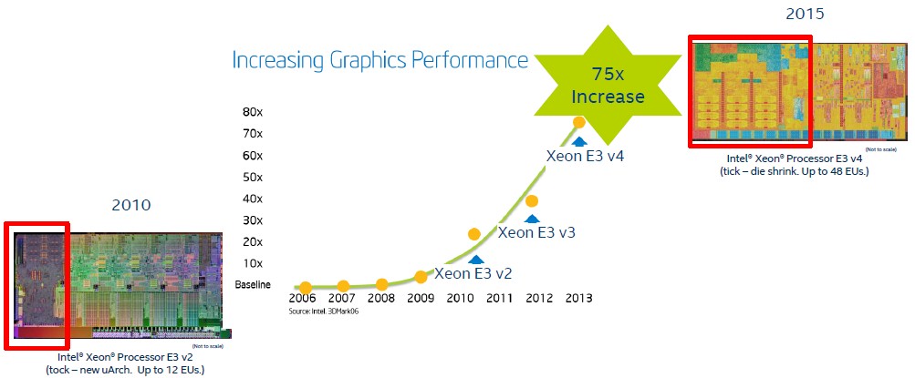
A big part of the Broadwell Xeon E3 v4 story on the server front is the integrated graphics, and Intel is quite proud of the fact that it can cram ever-increasingly more powerful GPUs into the Xeon E3 chips and their Core i7 counterparts for desktop and laptop machines.
The on-die GPU used on the Broadwell Xeon E3s is about 75X faster than the on-package GPUs that Intel started weaving into high-end desktop and low-end server parts back in 2008. The die shrink to 14 nanometers with the Broadwell parts and holding the core count steady at four allows Intel to add a fairly beefy GPU to these Broadwell chips. And it did that, nearly doubling the GPU performance. The higher clock speeds on the cores used in the Broadwell Xeon E3s also means the CPU side is getting a nice performance boost, too.
Intel is telling customers who are doing video delivery that the Haswell Xeon E5-2600 v3 processors will deliver the highest video quality given their performance (even though they do not have integrated GPUs, and that is presumably with the caveat that some kind of GPU card is added to the system), while the Broadwell Xeon E3 v4 processors are optimized to give higher node density and therefore support more streams in a given space. The same math holds true for virtual desktop infrastructure streaming setups that have one dedicated node per remote end user, we presume.
According to benchmark tests done by Intel, a rack of Supermicro SuperServer microservers with a dozen sleds in a 3U enclosure can support 4,368 concurrent video streams of HD video per rack using the Broadwell Xeon E3-1285L v4 processors. The same setup using the Haswell Xeon E3-1285L v3 chips could pump 3,120 HD streams. That is a 40 percent increase in video streaming performance moving from Haswell to Broadwell.
We would love to know what kind of floating point performance that Iris Pro Graphics P6300 has and how it might be used to accelerate other kinds of workloads. Intel is not pitching the on-die GPU in this fashion, but that won’t stop some clever hacker or researcher from trying. We hope, anyway.

Intel Is Counting On AI Inference To Save The Xeon CPU
There is little question that generative AI as well as other kinds of machine learning are going to augment applications in every industry and in every part of the application stack in the coming years. It is also pretty obvious that AI training for the most advanced models, with trillions …
One New Feature For Intel’s HPC Compute Engines: Contrition
It is very rare for any of the major semiconductor suppliers of the world to ever admit that things are going wrong, even when we all know that they have been. But as part of a briefing ahead of the SC22 supercomputing conference next week and just ahead of AMD’s …
Intel To Amp Up Security With “Ice Lake” Xeon SP Servers
Security is one of those necessary things that should not be an afterthought, but often is, and ideally is so invisible that it doesn’t get in the way of applications and the infrastructure it runs on. Speaking very generally, the cost of security has been so high on servers that …
I think it would be interesting if they made an E3 Xeon with an integrated FPGA in place of the GPU and with a large shared L4 eDRAM cache on the package or die itself.
Any specifics on how much the eDRAM actually speeds up CPU performance when there’s a discrete GPU and its just acting as an L4 cache?
This server has Intel inside. The HP Proliant ML350 G9 rack server: https://www.youtube.com/watch?v=vdamv56LQio