

A new CPU or GPU compute engine is always an exciting time for the datacenter because we get to see the results of years of work and clever thinking by hardware and software engineers who are trying to break through barriers with both their Dennard scaling and their Moore’s Law arms tied behind their backs. Such is the case with the “Ampere” GA100 datacenter GPU that Nvidia launched today.
But ultimately, what is interesting is how these devices are used in systems and then lashed together into clusters, and given Nvidia’s increasing focus on the datacenter, which we discussed at length a few weeks ago with Nvidia co-founder and chief executive officer Jensen Huang, the systems it designs and sells itself are indicative of how it believes its GPU compute engines should be deployed in DGX, HGX, and now EGX systems for the datacenter and for the edge. (Think of the edge as a massively distributed and loosely coupled datacenter, which we certainly do.)
Without further ado, let’s start with the new DGX A100 system, and you will note that Nvidia has done away with the number designation for its DGX server generations – it is not called DGX 3 – and is just tagging it with the Tesla accelerator name at the end, thus avoiding confusion as we had with DGX 1 machines that started with “Pascal” GP100 accelerators and then had “Volta” GV100 accelerators added two years later but Nvidia did not do anything to designate that motor change. Now, as you would expect from a car aficionado like Huang, the motor is now the designation for the system. Which is logical.
The DGX A100 scales up to only eight GPUs, and it is our guess that the NVSwitch at the heart of the system has had its port bandwidth reallocated to handle the doubled up bandwidth (600 GB/sec for the Ampere A100 across all six of its NVLink ports versus 300 GB/sec for all six ports on a Volta V100); with the same aggregate switching bandwidth, you can only have half as many ports at twice the bandwidth, and hence the drop in scale from sixteen GPUs in a single NVLink image to eight GPUs. That is not to say that Nvidia could not goose the NVSwitch to scale to sixteen or even higher GPU counts, but we also think that maybe NVSwitch was really designed for the Ampere generation and, as Nvidia has said in the past, got pulled into the market early for the Volta generation.
With the acquisition of Mellanox Technologies, suffice it to say that Nvidia has all kinds of things it can – and will – do with interconnects.
Here is the exploded view of the DGX A100 system:
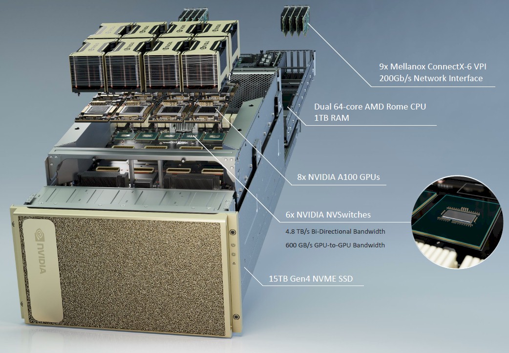
The first interesting thing to notice, aside from the new GPU accelerator of course, is that unlike the prior DGX-1 and DGX-2 systems that were based on Intel Xeon E5 and Xeon SP hosts, this one has a two-socket node based on AMD’s “Rome” Epyc processors. To be precise, the underlying host has a pair of 64-core Epyc 7742 top bin parts, which have a base clock speed of 2.25 GHz and a boost clock speed of 3.4 GHz. AMD won the CPU deal, according to Charlie Boyle, vice president and general manager of the DGX systems business, for two reasons: The PCI-Express 4.0 support and the high core count of 128 cores. Intel’s latest “Cascade Lake-R” Xeon SP processors top out at 28 cores and only support PCI-Express 3.0, which is not really enough to drive 200 Gb/sec InfiniBand ports in the numbers that the DGX A100 system has.
This CPU host system has 1 TB of main memory (it could host as much as 4 TB if customers needed it to, but that would be very pricey indeed). The system runs the Ubuntu Server variant of Linux from Canonical, and two 1.92 TB M.2 NVM-Express memory sticks are used to host that operating system. The machine had four 3.84 TB U.2 NVM-Express flash drives for local storage for a total of 15.4 TB of capacity. The system is equipped with a total of nine ConnectX-6 VPI network interface cards. One implements Ethernet running at 200 Gb/sec (or slower) Ethernet to connect to the outside world and the other eight are supporting 200 Gb/sec Quantum HDR InfiniBand, which are used to cross-couple DGX A100 systems together to run clustered HPC and AI workloads at very high bandwidth (1.6 Tb/sec aggregated). It obviously takes a lot of switching to pod up dozens and hundreds of these DGX A100 systems, and now you begin to see why Nvidia bought Mellanox.
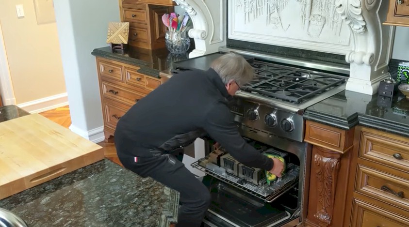
Most of the 6U of vertical space in the DGX A100 machine is used to house the motherboard and the NVSwitch backplane for the eight Tesla A100 SXM2 modules together, which weigh in at 400 watts a piece. Here is Huang taking the first one out of the oven in his house after baking it for what we presume was a few years:
That NVSwitch backplane has 4.8 TB/sec of bi-directional bandwidth lashing them together into what is effectively a shared memory NUMA GPU complex. While they are not shown in the diagram, there has to be a complex of PCI-Express switches to interlink the GPU complex with the host CPU complex.
This GPU and NVSwitch complex is called the HGX A100 when it is outside of the system, and it is sold to OEM and ODM partners as a single unit rather than in piece parts as Nvidia did with earlier HGX components that were sold for hyperscaler and public cloud deployments (and sometimes not using the SXM2 socket and NVLink interconnect, but the PCI-Express variants of the HGX motherboards, which were obviously cheaper but also package about a tenth of the bi-section bandwidth as the NVLink version.)
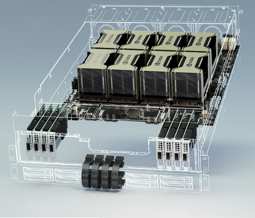
This HGX A100 assembly weighs around 50 pounds all by itself. Huang says that Nvidia is selling this as an integrated system because it has over 1 million drill holes, which all have to be done precisely, plus over 30,000 components and an over 1 kilometer of wire traces between those components; it has copper heat removing pipes all over the place, which have to be perfectly configured to work properly.
“It is the most complex motherboard in the world,” Huang explains, and when he took it out of the oven he said it was the largest GPU in the world. Both are true statements, and yes, you can play a hell of a lot of Crysis on it – if you can get Crysis to run on Linux in the WINE emulator, that is.
Both the HGX A100 GPU complex and the full-on DGX A100 system have been in full production “for some time now,” according to Huang. All of the clouds already have HGX units so they can deploy, and this includes Alibaba Cloud, Amazon Web Services, Baidu Cloud, Google Cloud, Microsoft Azure, Oracle Cloud, and Tencent Cloud. And all of the key server OEMs, including Atos, Cray, Dell, Fujitsu, Gigabyte, Hewlett Packard Enterprise, Inspur, Lenovo, Quanta Computer, and Supermicro are all in the pattern, too. But they will take a few weeks to months (excepting Supermicro, of course, which always gets out the door first on announcement day) to bring their own variants of the DGX A100 to market.
The DGX A100 system delivers 10 petaops of peak INT8 performance (used for inference mostly) and 5 petaflops of peak half precision FP16 performance. Using the new Tensor Flow32 format created by Nvidia, which we explained here, the system delivers 2.5 petaflops aggregate peak including the 2X acceleration for sparse matrix math; this is a factor of 16X higher than the peak 156 petaflops FP32 that the plain vanilla FP32 units on the Ampere GPU delivers. (Which makes us wonder why the regular FP32 units are there, but backwards software compatibility has to be maintained.) For floating point math, the regular FP64 units deliver 9.7 teraflops of double precision oomph, but the new Tensor Cores can also now do 64-bit math and they can deliver 19.5 teraflops, for a peak of 156 teraflops across the DGX A100 complex using the tensor cores or 77.6 teraflops using the regular FP64 units. (We wonder how many of these execution units can be used concurrently. We will find out next week.)
To a certain extent, Nvidia is a server maker because it is one of the largest AI and HPC users in the world, designing its chips and creating AI software stacks and tools that it not only uses to design its wares, but also to distribute as software stacks that Nvidia’s customers then use to implement AI and HPC applications. It is a virtuous cycle. But it also means that Nvidia has to itself invest in DGX systems and switching to link it together (again, another reason to buy Mellanox).
To that end, Nvidia is creating a new SuperPOD configuration that the company can itself use and also allows it to sell supercomputer chunks to external customers. The DGX A100 SuperPOD has 140 of the DGX A100 systems, with a total of 1,120 of the Tesla A100 GPU accelerators), all linked together with 170 HDR InfiniBand switches from its Mellanox unit, delivering 280 TB/sec of network fabric bandwidth across 15 kilometers of optical cables. This updated SuperPOD has 700 petaflops of “AI performance” and can be built in three weeks.
Before the Ampere launch today, the in-house Saturn V supercomputer that Nvidia runs has been extended with the new Ampere SuperPOD. In fact, the system has had four of these SuperPODs added, and here is a space age picture of the Nvidia datacenter:
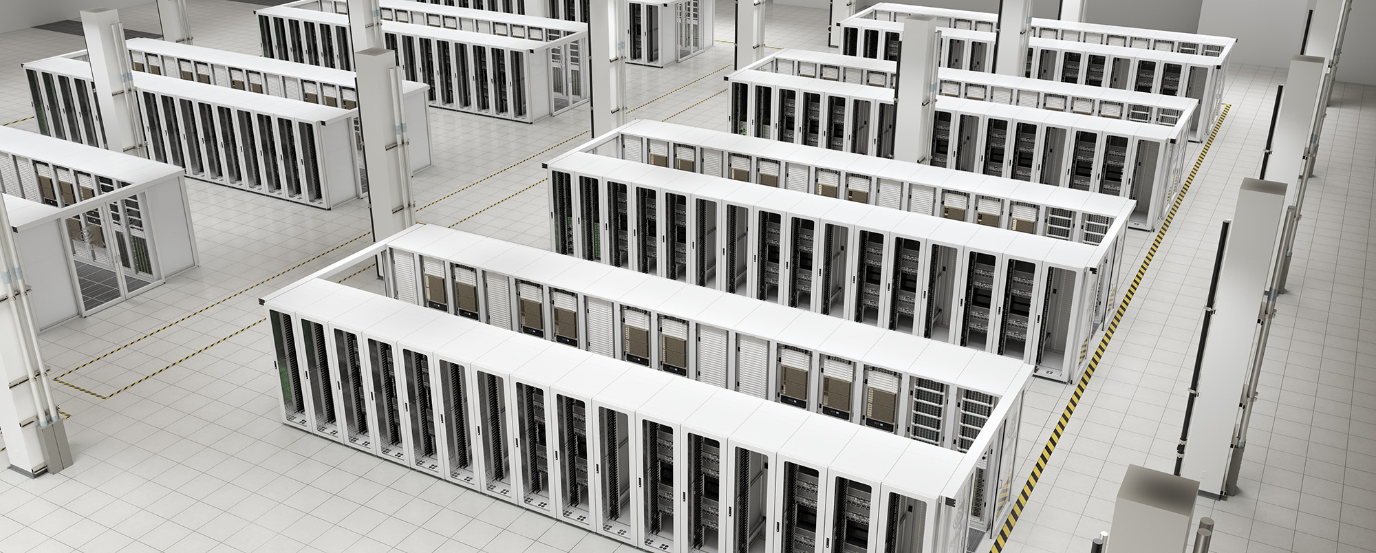
Before the expansion, three different generations of DGX machines that comprised the Saturn V supercomputer had 1,800 DGX machines with a total of 1.8 exaflops of that “AI performance” and the four SuperPODs based on the DGX A100, with a total of 560 machines, will add another 2.8 exaflops for a total of 4.6 exaflops. Huang said that there are maybe four or five other companies in the world that have more AI oomph than this. (You will notice that the racks are not even close to half full. Wherever this datacenter is, real estate is not as big of a problem as power density.)
The DGX A100 system costs $199,000, We are not doing a full price/performance analysis right here, but the DGX-1V (we put the V in there for Volta) cost $149,000 and had anywhere from a third to a twentieth of the performance, depending on the data format, while the much heftier DGX-2 with NVSwitch came closer in performance but also cost $399,000. The DGX A100 will blow the prior DGX-1 and DGX-2 systems out of the water, plain and simple. (We will be doing the bang for the buck math in detail in a follow-up story.)

Strong-Armed Into HPC, Like It Or Not
If you are an HPC center in Europe, and particularly one that is funded by public funds, you are thinking about Arm-based CPUs in your supercomputers. And that is despite Arm Holdings being a British company and all of the issues with the United Kingdom and its Brexit separation from …
AMD Is Beating Nvidia At Its 2017 Game, But The Game Has Moved On
Hold on a second. Nvidia’s sales of chips and systems to supercomputer centers are not as big as we might be thinking. Not even close. Nvidia may have pioneered the idea of GPU acceleration for HPC simulation and modeling applications. It may have supplied the vast majority of the compute …

Hot On The Heels Of Mellanox, Nvidia Snaps Up Cumulus Networks
Last week, when we talked to Nvidia co-founder and chief executive officer, Jensen Huang, about how the datacenter was becoming the unit of compute and in such a world networking was critical, it was obvious that acquiring Mellanox Technologies for $6.9 billion was just the beginning of the strategy that …
In 2034 the playstation 7 will have that same power… And we will all live in the Matrix in 8K VR 240hz!
Why doesn’t Nvidia use IBM POWER CPUs in their DGX servers? Are the host CPUs that unimportant?
With POWER9 scale up they could have 8TB in 2 sockets and have NVLink on the CPUs as well with no PCIe switches needed.
It is a good question, and I suggested that a few years back. I think IBM wants to sell its own AC922 and the wonder is why there are not larger and fatter Power Systems machines with NVSwitches. Gotta figure IBM doesn’t think there is margin in that, but I can’t imagine that this is correct. The other thing is that using Power9 chips would mean burning some of the NVLink ports for the GPU interconnect on the CPU-GPU interconnect, and that would reduce the GPU count in a single image. Maybe NVLink 2.0 is not as important for hosts as is PCI-Express 4.0 and PCI-Express switches to link CPUs to GPUs is, in fact, good enough.
the main problem with NVIDIA is the ecosystem…and vendor lockin. If you get into it will be a nightmare to get out. New and better approaches will come and you’ll stuck with your CUDA directives…
“and you will note that AMD has done away with the number designation for its DGX server generations” -> I think AMD should read Nvidia here?
Very exciting times we are living in for HPC :).
Good article!
<> Yup.
Without further ado, let’s start with the new DGX A100 system, and you will note that AMD has done away with the number designation for its DGX server generations
Please fix typo 🙂 (yes, i work for nvidia, but am not involved on any PR / marketing, i read this website purely out my own interest)
Deepest apologies. I was thinking about the CPU. Moving fast.