

Intel has the kind of control in the datacenter that only one vendor in the history of data processing has ever enjoyed. That other company is, of course, IBM, and Big Blue wants to take back some of the real estate it lost in the datacenters of the world in the past twenty years.
The Power9 chip, unveiled at the Hot Chips conference this week, is the best chance the company has had to make some share gains against X86 processors since the Power4 chip came out a decade and a half ago and set IBM on the path to dominance in the RISC/Unix market.
IBM laid out a roadmap out past 2020 for its Power family of processors back at the OpenPower Summit in early April, demonstrating its commitment the CPU market with chips that are offer a brawny alternative to CPUs and accelerators compared to the Xeon and Xeon Phi alternatives from Intel and the relatively less brawny chips from ARM server chip makers such as Applied Micro and Cavium and the expected products from AMD, Broadcom, and Qualcomm. We pondered IBM’s prospects in the datacenter in the wake of some details coming out about next year’s Power9 processors, which IBM said at the time would come in two flavors, one aimed at scale-out machines with one or two sockets and another aimed at scale up machines with NUMA architectures and lots of sockets and shared memory.
As it turns out, IBM will be delivering four different variants of the future Power9 chip, as Brian Thompto, senior technical staff member for the Power processor design team at the company, revealed in his presentation at Hot Chips. There was only one Power7 and one Power7+, with variants just having different cores and caches activated. There were three Power8 chips, one with six cores aimed at scale out workloads and with two chips sharing a single package and one single-die, twelve-core chip aimed at bigger NUMA machines; this year saw the launch of the Power8 chip (not a Power8+ even though IBM did call it that for some time) with twelve cores with the NVLink interconnect from Nvidia woven into it.
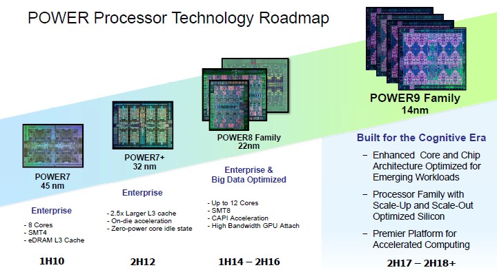
With the Power9 chip, there will be the Power9 SO (short for scale out) variant for machines aimed at servers with one or two sockets, due in the second half of 2017, and the Power9 SU (short for scale up) that will follow in 2018 for machines with four or more sockets and, we think, largely sold by IBM itself for its customers running its own AIX and IBM i operating systems.
The four versions of the Power9 chip differ from each other in terms of the number of cores, whether or not the systems have directly attached memory or use the “Centaur” memory buffer chips, and level of simultaneous multithreading available for specific server configurations, as shown below:
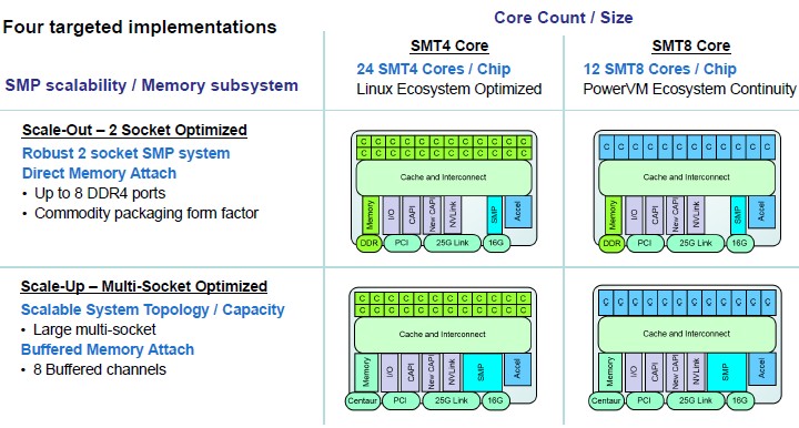
The twist on the SMT level is the new bit we did not know, and we also did not know the core counts that would be available on the Power9 SU variants. We knew that the Power9 SO chip would have 24 cores, and by the way, Thompto tells The Next Platform that the Power9 SO chip is a single die chip with 24 cores. The Power9 SU chip will top out at twelve cores, just like the biggest Power8 chip did. Both Power9 chips have eight DDR memory ports, each with its own controller on the die, which now can either talk directly to two DDR memory sticks on the Power9 SO or to a Centaur buffer chip that in turn talks to four DDR memory sticks each.
Thompto said that the Power9 SO chip has 120 GB/sec of sustained memory bandwidth with lower latency than was possible with the buffered memory setup with the Power8 and with the Power9 SU coming out in 2018. The Power9 SO chip aimed at the commodity two-socket server space where Intel’s Xeon E5 chips rule can use the same commodity DDR4 memory sticks, and the Power9 SO will come in a commodity form factor packaging that is more like the Xeon E5 than the current Power8. Architecturally, Thompto says that the Power9 SO can support a maximum of 4 TB of main memory using 256 GB memory sticks, but practically speaking, using 64 GB memory sticks the capacity will top out at 1 TB for these systems.
The Power9 SU machines, on the other hand, will have eight buffered channels and have up to 8 TB of main memory available across the 32 memory slots each socket can support, provided customers can afford 256 GB sticks. Again, 2 TB per socket is the practical, economic limit for memory for most customers. That buffered memory also implements an L4 cache on the Centaur chip, and also implements chip kill and lane sparing, and will be compatible with existing Power8 memory cards, which is something Big Blue’s existing Power Systems customers will like to hear. The extra RAS features and the 230 GB/sec of sustained memory bandwidth per socket is also a key differentiator for the Power8 and Power9 SU chips, and something that IBM no doubt wishes it were possible to bring down to the Power9 SO. But that would have necessitated putting sixteen DDR4 ports on the Power9 SU chip for a total of 32 memory sockets, and for whatever reason, IBM did not do this.
In addition to the different core counts and memory options, IBM is making the Power9 SO and Power9 SU chips available with two different levels of simultaneous multithreading, SMT4 with up to four virtual threads per core and SMT8 with up to eight virtual threads per core. IBM already supports SMT8 with the Power8 chips, and backstepping to SMT4 for versions of the chips may seem like an odd choice. But according to Thompto, the Power9 SMT4 chips are designed with a focus on Linux systems that want high core counts and that want to have the most granularity for server virtualization, while the Power9 SMT8 chips are optimized for large logical partitions with IBM’s PowerVM hypervisor and for workloads that need more threads rather than stronger threads.
This would suggest that the SU chips will have fewer cores and higher clocks, as we suspected back in April, while the SO chips will have more cores but lower SMT levels and presumably lower clocks. But, just for fun, there is an SU chip that will have 24 cores and the SO chip will be available in a twelve-core variant, too, just in case there are workloads that will go in different directions.
Drilling Into The Core
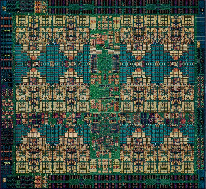
The Power9 chip is a biggie, weighing in at 8 billion transistors. It is made using the 14 nanometer FinFET manufacturing processes from Globalfoundries, which acquired IBM’s fab business two years ago (the 14HP process, to be specific). This process has 17 layers and significantly makes use of the embedded DRAM (eDRAM) memory perfected by Big Blue in the Power7, Power7+, and Power8 chips to create a 120 MB shared L3 cache for all of the cores on the Power9 SO die.
Here is what the Power9 SO die looks like:
And here is what it looks like when you block off its main components:
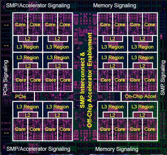
IBM did not provide a die shot or block diagram of the twelve core variants of the Power9 SU and Power9 SO chips, but they don’t really have that much of a different size and layout for the transistors because of the way the fat SMT8 and skinny SMT4 cores have been created using what IBM calls an execution slice microarchitecture.
“We started with a 64 bit compute building block and we coupled that with a 64 bit load store building block,” explained Thompto. “Each compute building block has a heterogeneous mix of compute, fixed and float, supporting scalar and vector. This allows us to obtain high utilization of our compute resources while also providing seamless exchange of data and shared data paths. It also serves as an efficient building block for managing instruction flow through the machine. We couple two of these 64 bit slices together to make a 128 bit superslice, and this is our physical design building block.”
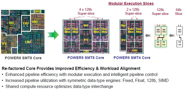
Two of these superslices comprise an SMT4 core, and four of them comprise an SMT8 core, and Thompto says that the Power9 pipeline was shorter from fetch to compute by five cycles compared to the Power8 core and had better branch prediction. The SMT4 core can do 64 instructions per cycle and the SMT8 core can do twice that at 128 instructions per cycle. The end result of all of the tweaks in the microarchitecture is a leaner and stronger core. Here are the feeds and speeds of the Power9 SMT4 core:
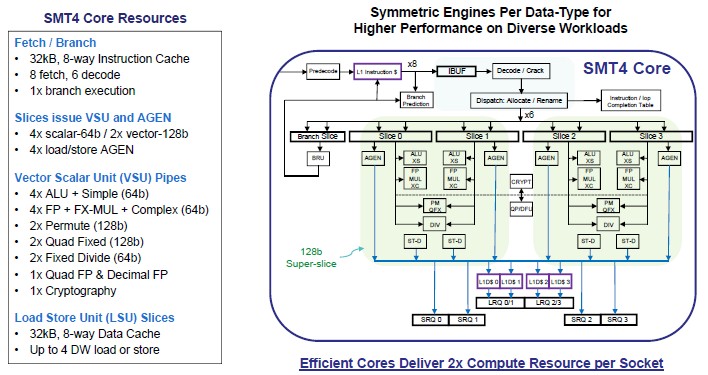
The Power9 chip is the first chip from IBM to support the Power 3.0 instruction set, which has a number of tweaks to it. First of all, the new ISA definition supports 128-bit quad-precision floating point math that is compliant with the IEEE 754 standard and, importantly, is useful for certain financial services and security applications that require higher precision floating point math. The new ISA also supports 128 bit decimal integer math, which is useful with databases and anything that is doing money math. IBM has also added a single-instruction random number generator, which is important for all kinds of simulations that require lots of randomness (it took more than one cycle to do this with the Power8 chips). There are a slew of other nips and tucks, including hardware assisted garbage collection for Java, PHP, and other interpreted languages and a new interrupt architecture that will make highly virtualized environments (presumably both OpenKVM and PowerVM hypervisors) run more smoothly.
The Power9 chip with the SMT8 cores are aimed at analytics workloads that are wrestling with lots of data, in terms of both capacity and throughput. The 24 core variant of the Power9 with SMT8 has 512 KB L2 cache memory per core, and 120 MB of L3 cache is shared across the dies in 10 MB segments with each pair of cores. The on-chip switch fabric can move data in and out of the L3 cache at 256 GB/sec, and adding in the various interconnects for memory controllers, PCI-Express 4.0 controllers, and the “Bluelink” 25 Gb/sec ports that are used to attach accelerators to the processors as well as underpinning the NVLink 2.0 protocol that will be added to next year’s “Volta” GV100 GPUs from Nvidia and IBM’s own remote SMP links for creating NUMA clusters with more than four sockets, and you have an on-chip fabric with over 7 TB/sec of aggregate bandwidth.
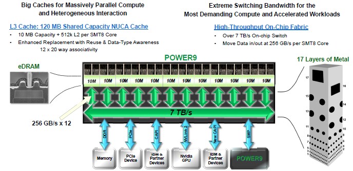
The Power9 chips will have 48 lanes of PCI-Express 4.0 peripheral I/O per socket, for an aggregate of 192 GB/sec of duplex bandwidth. In addition to this, the chip will support 48 lanes of 25 Gb/sec Bluelink bandwidth for other connectivity, with an aggregate bandwidth of 300 GB/sec. On the Power9 SU chips, 48 of the 25 Gb/sec lanes will be used for remote SMP links between quad-socket nodes to make a 16-socket machine, and the remaining 48 lanes of PCI-Express 4.0 will be used for PCI-Express peripherals and CAPI 2.0 accelerators. The Power9 chip has integrated 16 Gb/sec SMP links for gluelessly making the four-socket modules. In addition to the CAPI 2.0 coherent links running atop PCI-Express 4.0, there is a further enhanced CAPI protocol that runs atop the 25 Gb/sec Bluelink ports that is much more streamlined and we think is akin to something like NVM-Express for flash running over PCI-Express in that it eliminates a lot of protocol overhead from the PCI-Express bus. But that is just a hunch. It doesn’t look like the big bad boxes will be able to support this new CAPI or NVLink ports, by the way, since the Bluelink ports are eaten by NUMA expansion.
The bandwidth improvement with this new CAPI and NVLink 2.0 running atop Bluelink is impressive. Moving from a PCI-Express 3.0 x16 slot to one using PCI-Express 4.0 doubles up the peak bandwidth, says Thompto, and adding NVLink to the Power8 chip with four ganged up NVLink 1.0 ports boosted the bandwidth between the processor and a “Pascal” Tesla P100 GPU by 5X. With the Bluelink ports, the bandwidth between the Power9 chip and accelerators will be anywhere from 7X to 10X higher, depending on the accelerator and the protocol.
So how will the Power9 chip perform? It depends on the workload. Take a look:

In the comparison above, IBM is comparing a Power8 chip with twelve cores using SMT8 threading running at 4 GHz to a Power9 chip with the same clock speed, core count, and threading. In this case, performance increases range from a low of around 50 percent to a high of 125 percent. It will be interesting to see how the different clock speeds, thermals, SMT levels, and memory bandwidth all add up to different performance across the Power9 line and compared to Xeon, Opteron, and ARM alternatives coming to market next year.
2017 is gonna be a lot of fun for server processors. That much we know for sure. We will be drilling down into the system options for the Power9 chips in a follow-on story.


impressive chip! 50% to 125% (more than 2x) w.r.t. previous generation. The innvoation in the microarchitecture made this possible. Great move by IBM, not like Intel that did no show anything new in microachitecture for the last 6th generations, with diminishing perf improvements. Let’s see what happen next year! very interesting!
“…impressive chip! 50% to 125% (more than 2x) w.r.t. previous generation….”
If you consider the Oracle SPARC M7 from last year is 2-3x faster than POWER8 and Intel Xeon, all the way up to 11x faster socketwise – it means POWER9 is slower than current SPARC M7. POWER8 is also slower than Intel Xeon which means POWER9 will (probably) catch up on Intel Xeon. I dont really consider POWER9 impressive in light of this?
Next year Oracle will release SPARC M8 cpu, and we all know that new Oracle SPARC cpus are at least twice as fast as the previous generation. Oracle has released six SPARC cpus in six year, so it is time for SPARC M8 next year. Which again will be (at minimum) 2x faster than SPARC M7.
Posting information I’ve posted before, to counter a well-known Oracle shill…
Per SPEC, 32-core SPARC M7 is about 30% faster at integer performance than 12-core Power8 (900 vs 1200 SPECint_rate/socket.) Not 2-3x. Oracle has *not* doubled per-socket performance every year (they certainly didn’t this year, as they only launched a low-end chip that wasn’t twice as fast as any obvious predecessor.) T4 wasn’t twice the throughput of T3 – in fact, it was about the same amount of throughput, but higher ST and single-core performance. Oracle’s own roadmap, found at http://2eof2j3oc7is20vt9q3g7tlo5xe.wpengine.netdna-cdn.com/wp-content/uploads/2014/04/oracle-sparc-roadmap-2014.jpg, shows the next-generation SPARC only increasing throughput by 30%.
For anyone who hasn’t had the pleasure of reading this guy’s comments, I highly recommend getting a few teaspoons of salt and looking up “Kebabbert” and “Brutalizer”.
Well, you are correct in that SPARC M7 is only 30% faster than POWER8 in SPECint2006, not 2-3x faster. This SPEC2006 benchmarks is probably the worst benchmark for SPARC M7, it is only 30% faster than POWER8.
Other benchmarks (not SPEC2006) are typically 2-3x faster, all the way up to 11x faster. If we look at the 30ish SPARC M7 benchmarks here:
https://blogs.oracle.com/BestPerf/entry/20160629_jbb_sparc_s7_2
It is likely that on average, SPARC M7 is 2-3x faster than POWER8 because for instance, SPARC is 11x faster on databases, which more than makes up the bad SPEC2006 result. So if we average all those 30ish benchmarks, SPARC M7 is 2-3x faster than POWER8. And these benchmarks range from neural networks, databases, SAP, STREAM RAM bandwidth, virtualization, Machine Learning, Hadoop, etc etc. So it is a very wide range of workloads. And if we just narrow it down to business ERP workloads, such as SAP, databases, etc – there is no contest. SPARC M7 is built for that kind of workloads, and it is way faster than any other cpu on the market.
So when I said M7 is 2-3x faster, I did not mean it is 2-3x faster on every benchmark. I meant on average: some benchmarks it is 11x faster, other benchmarks, 5-6x faster. The worst case is SPEC2006, where it is only 30% faster.
.
You are wrong again. Oracle has doubled performance every year. In your roadmap you showed us, we see that SPARC T4 has 5x single threaded performance, and same throughput as T3. This makes the total performance increase (thread performance times throughput):
SPARC T4 = 5 thread performance x 1 throughput = 5x
SPARC T5 = 2.5 x 1.2 = 3x
SPARC M5 = 6 x 1.5 = 9x
SPARC M6 = 2 x 1 = 2x
SPARC M7 = 2 x 1.5 = 3x
And now Oracle talks about SPARC M8, which will have 30% better thread performance than SPARC M7, and 50% better throughput. This means SPARC M8 is 1.3 x 1.5 = 1.95x faster than SPARC M7. So you are wrong on this too.
Regarding the new SPARC S7, it is a crippled version of M7. It is a 8-core version of SPARC M7. The purpose is for customers wanting few cores (because of licensing) and scale-out servers. But make no mistake, the SPARC S7 cores are the same as SPARC M7 cores – which means they are typically 2x faster cores than POWER8 or Intel Xeon.
.
Regarding this POWER9. It seems that on average, it will be 75% faster than POWER8. In best case POWER9 is 2.25x faster than POWER8 on Graph Algorithms. Well, we know that Intel Xeon is faster than POWER8, and SPARC M7 is 2.1 – 2.7x faster than Intel Xeon on Graph Algorithms. https://blogs.oracle.com/BestPerf/entry/20160629_pagerank_t7_4
On average SPARC is 2.475x faster than Intel Xeon. This means that POWER9 will be slower than last year’s SPARC M7.
.
I dont really understand the point of IBM releasing slow cpus, and hail it as the fastest cpu ever? Even Intel Xeon is faster today. POWER is worst in class. Soon even ARM probably will beat POWER, as it already has in Performance/watt.
If you really do claim that POWER8 is faster than SPARC M7, then you are welcome to show us any benchmark where POWER8 beats SPARC M7. Can you show us one single benchmark? No? Ok, can you show us a single benchmark where Intel Xeon beat SPARC M7? No? Fine, so we can all conclude that SPARC M7 is the fastest cpu in the world then. So when you call me a Troll and Shill for posting benchmarks, the only important thing is really the hard numbers and facts, right? Instead of name dropping, show us benchmarks to back up your claim. Scientific method is proving your claims, otherwise it is just wishful thinking in best case. And in worst case it is FUD.
I am incapable of understanding how someone like you can become this delusional. This is… this is random, arbitrary, incomprehensible crap. It’s not worth trying to even decipher half of what you said to debunk it. If anyone’s spreading FUD it’s you with random jargon-tier crap.
That is possibly the most bizarre interpretation of performance numbers I’ve ever read. “Throughput” in the roadmap is not to be multiplied by “thread strength.” It fairly clearly refers to performance per socket, while “thread strength” refers to ST perf.
T4 ramped up clocks and went to a wider, out-of-order core, so ST perf went through the roof. Core count got cut in half, so throughput didn’t. This is not a hard concept to understand.
Not even going to touch the rest, but will simply note that this kind of trash is why my company doesn’t develop for SPARC.
Oh wait, the SPARC marketing troll! 😛
I have not seen anything about SPACE on #Hotchips . Honestly, SPARC is dying, and Oracle will switch to Intel eventually. It is a matter of time. Only big machines, a diminishing small market niche, use sometimes SPARC…
@nopony,
You claim it is not possible to multiply thread and throughput performance. You say something like “when thread performance has increased 30% it also explains the 50% increase in throughput, so it is not possible to 1.3 x 1.5 = 1.95. No, instead cpu performance has only increased 30%”.
You equate thread performance with throughput: “thread performance = throughput”. This is wrong to do. There is no equivalence. Instead, it looks like this: “thread performance => throughput”.
So what happens if you only increase throughput? Does that also increase thread performance? No. Say IBM doubles the number of cores, but thread performance stays the same. Then the cpu performance as a whole has been doubled as the workloads can be twice as large. So you must multiply thread and throughput performance. You can not claim that this IBM cpu performance has not increased at all, because “thread performance stays the same”.
Actually, this concept is not as difficult as you think. Just think over this example a bit. Workload performance are determined by thread performance times throughput. Those concepts are orthogonal in one direction. In that case you must multiply thread times throughput to assess the cpu performance.
Oracle has been clear “they increased thread performance X% and also increased throughput Y%”. This means the workloads that can be handled are greater than if only thread performance was increased. Just contemplate this a bit, it is not as difficult as you think it is.
Well, I don’t know any customer in commercial, enterprise computing space that runs *any* workload that is comparable to the SPEC CPU2006 benchmark. Its a very outdated, now 10-years old benchmark that doesn’t test the OS, nor any application or database and doesn’t even involve I/O testing. There is no workload in todays world that shares commonality with SPEC CPU2006. SPEC CPU2006 is also easily optimized to hide NUMA architecture limits and why you see near linear scaling results to 100’s of cores which clearly doesn’t make sense.
There are a multitude of other benchmarks out there, based on newer, even latest workload standards like SPECjbb2015, SPECvirt_sc2013, SPECjEnterprise2010 and even the HammerDB open source testing tool that simulates TPC-C/OLTP workload. Theres even application level benchmarks like SAP SD 2-Tier, Siebel, Peoplesoft, Oracle E-Business Suite, etc.
Three independent benchmarks I like looking at is SPECjbb2015, SAP SD 2-Tier and HammerDB. The SPECjbb2015 benchmark is brand new and fully tests JAVA Server performance, while the SAP benchmark has been around a while too but continuously gets improved with newer versions. Anyone can run the HammerDB test on any Database, so it’s a great tool for verifying Database OLTP performance.
Oracle released SPARC T7-1 results, achieving 120,603 SPECjbb2015-MultiJVM max-jOPS and 60,280 SPECjbb2015-MultiJVM critical-jOPS. Whats interesting is the critical-jOPS test which measures critical throughput under service-level agreements (SLAs), with response times ranging from 10 to 100 milliseconds.
While IBM did publish previous SPECjbb2013 results on its high end E870, as well as Power S824, SPEC discovered that SPECjbb2013 could be vendor optimized, providing false results and so was fixed with the newer SPECjbb2015. Almost 2 years later, IBM has only released results on its smallest IBM Power S812LC achieving 44,883 SPECjbb2015-MultiJVM max-jOPS and just 13,032 SPECjbb2015-MultiJVM critical-jOPS.
So Oracles single SPARC M7 SPARC T7-1 system achieves 2.7x faster max-jOPS and a whopping 4.6x faster critical-jOPS than the single Power8 based S812LC system, highlighting that throughput and more importantly, response times matter.
And just recently, Oracle released SPARC M7-8 SAP results. With just 8 x SPARC M7 CPUs, the system achieved 130,000 SAP Users. IBM’s only Power8 enterprise result shows a IBM Power System E870 (MME) with 8x Power8’s @ 4.19GHz achieving 79,750 SAP users. The SPARC M7 supports 1.63x more Users/CPU than Power8.
And finally, running the HammerDB OLTP test, a SPARC T7-1 with just one SPARC M7 CPU achieves 4,938,629 TPM/chip. IBM ran the same test with the Power S824, with 2 x DCM’s, each having 2 x Power8’s @ 3.52GHz ( 4 x Power8’s total) achieving 902,458 TPM/chip. The SPARC M7 is 5.5x faster per CPU than the fastest Power8 @ 3.52GHz available in the S-Series.
So as you can see from just these 3 public benchmarks, SPARC M7 ranges from 1.63x to 2.7x to 5.5x faster than IBM’s Power8 today. And these benchmarks didn’t run/use the SW in Silicon technologies built in to SPARC M7.
Edison Group Labs, an independent testing company, tested SPARC M7’s SW in Silicon and in-memory capabilities comparing against IBM’s Power8 and Xeon, and they discovered SPARC M7 has up to 49x higher Data transfer Bandwidth than Power8 and so delivers about 4.3x more performance/CPU for unstructured big data workloads. http://www.oracle.com/us/solutions/oos/database/edison-oracle-software-in-silicon-2971285.pdf
Thus sayeth Phil with Oracle Marketing. Thank you Phil. When are you going to bring a M7 server to where I am to conduct a real live test benchmark against a POWER8 server? We will record and publish the results. Can’t wait to see these 3.3X and 49X results. You owe the world to see this comparison. Put up or please shut up. #BrokenRecord
These general up-to-date benchmarks confirms the picture of the SPARC M7 cpu, it is 2-3x faster than anything else on average. I prefer modern benchmarks to old, because modern benchmarks are harder to optimize for.
And that is why I dont really like those 49x data transfer bandwidth numbers. Sure, SPARC M7 achieves 600GB/sec when offloading data to the DAX database accelerators, whereas IBM POWER8 achieves 12GB/sec when offloading data to it’s CAPI accelerators which makes SPARC M7 around 49x faster.
But, I think those 49x numbers are just a sub part in the database benchmarks which makes SPARC M7 roughly 5x-11x faster than POWER8 in practice. So, I think it is better to look at the whole benchmark number instead of a tiny part. And at database benchmarks, SPARC is 5-11x faster in practice.
If you look at a tiny part, you can do as IBM does: look at the performance of a single core and extrapolate that number to the whole cpu. And we all know this is wrong to do. When we compare the fastest cpus, we need to look at the cpu benchmarks. Not core benchmark:
Core benchmark does not equate to cpu benchmark, which IBM wrongly claims.
Say you have one single core cpu achieving a score of 100, and you compete vs another cpu with 32 cores, each core achieving a benchmark score of 10.
IBM would say: “look, that single core achieves 100, therefore the cpu is fastest on the market!”
Other vendor would say: “Well, our cpu achieves a score of 320 in benchmarks, therefore our cpu is fastest on the market!”
Now, who is correct? IBM could claim “our core is fastest on the market” – which is a true statement. But IBM can not conclude that their entire cpu is fastest on the market, just by looking at one single core. And this is what IBM has been claiming all the time:
https://ibmadvantage.com/2013/04/29/weblogic-12c-on-oracle-sparc-t5-8-delivers-half-the-transactions-per-core-at-double-the-cost-of-the-websphere-on-ibm-power7/
“…[SPARC T5] Being “fastest processor in the world” means that such processor must be able to handle the most transactions per second per processor core…”
(Besides, SPARC M7 cores are faster than POWER8 cores and faster than Intel Xeon cores.)
SPARC is dead.
Oh, great. Phil the Oracle Marketing troll has a Mini-me.
Problem is that we can’t directly compare POWER8 vs SPARC M7 vs Xeon, because they all are aimed to different markets.
Xeons are well suited for HPC applications, they have large FPU which can be utilised by one thread using AVX 256/512. On the other hand, they are pretty bad for example in databases, because they have low memory bw and Intel is still not able to introduce working transaction support into x86.
SPARC M7 is completly differtly aimed product. They have impresive memory bw, lots of accelerators, crypto units… So they are great for big iron stuff and big databases, where they can achieve 20x per socket performance compared to Xeons. But they are not so good in HPC, where they can’t utilise all those extra stuff they have.
POWER 8 is somewhere between them. It is still big-iron but it seem that IBM is aiming at HPC applications. But they are not doing wery well because there is not so much SIMD code for POWER isa. And there are expensive memory buffers… I am curious, what POWER9 will look like in practice.
btw.: talking about single-thread performance is ridiculous:
1) They put 24-32 cores on single silicon not for single thread performance, but for maximum troghput.
2) Probably noone relizes, that higher “IPC” is achieved thanks to fact, that they put lots of resources under single core (Intel Haswell has 1024bit wide FPU, Skylake Xeons will have 2048 bit wide FPU!!!). But the only way to utilise it is using SIMD instructions. Try turn it off on your computer and it will perform simmilary like old 486.
But this is not problem, achieving better berformance thanks to paralelization is good, but aiming on single core/thread performance too much cowers real way where industry should go: SIMT (single instruction multipe threads).
@Jozo,
It is true that these cpus are aimed at different markets which makes comparison tricky. However, if you look at the 30ish benchmarks at
https://blogs.oracle.com/BestPerf/
you will see that the range is very diverse; from SPECcpu2006, neural networks, graph traversal, RAM bandwidth, virtualization, databases, SAP, big data hadoop, etc etc. And we do have benchmark numbers from x86 and POWER8 in the benchmarks as well. So, it is actually possible to compare all cpus because all run the same workload.
Sure, if there were nothing but database benchmarks on that Oracle web page, it would be silly because it is obvious that SPARC M7 is many times faster at database workloads than any other cpu. But, the benchmarks are well rounded. And in every single instance SPARC M7 wins. Typically it is 2-3x faster in all these very different workloads. (There are also benchmarks of SPARC S7, which is a crippled SPARC M7, but they share the same cores).
So, I would argue that it is possible to compare the cpus, by looking at their performance when they all run the same workload.
.
Regarding x86. Yes it is tailored to HPC because HPC code runs a tight for loop looping the same code on a few grid points over and over again. There is not much communication nor synchronization among the compute nodes, each run their computations almost in isolation. So the data is tiny and fits into the cpu cache. x86 is therefore first and foremost a desktop cpu, because desktops serve only one user which makes it possible to fit one user’s data into the cpu cache. That is why x86 cache design is very good, because the origin was to serve a single user. Single user cpus, i.e. desktop cpus, focus on a great cache design. They typically have low ram bandwidth and scale bad when you increase the number of cpus. POWER share the same traits as x86.
However, server cpus must serve thousands of users at the same time, and it is not possible to fit all those user’s data into a cpu cache, so servers dont focus on cache design because it is pointless. Instead, servers focus on great ram bandwidth, because the cpu needs to fetch the user’s data from RAM all the time. Also, when running Enterprise software, such as SAP or databases – there is lot of communication and synchronization going on all the time between the cpus, because ERP software are monolithic which means ERP workloads can not run in isolation on one single cpu. Scaling is a problem when running ERP software.
That is why you can not use clusters for Enterprise software such as SAP, because clusters are not fit for much communication between nodes. SGI UV2000 or UV3000 are basically a cluster, which is evident as all the use cases on SGI homepage is about HPC and no one has ever ran SAP nor databases on a large SGI server – because they are all HPC clusters in practice. You need to go to large 16-socket or 32-socket Unix servers for large ERP installations. Look at the top SAP benchmarks – it is all Unix. x86 does not scale, and also Linux scale bad. This is confirmed by SGI themselves, when they talk about why the UV2000 predecessor ALTIX clusters are not fit for ERP software, but only HPC clustered workloads:
http://www.realworldtech.com/sgi-interview/6/
Having good cpu cache is not important for server workloads, but ram bandwith is. That is why a single T5440 server with four 8-core 1.6GHz SPARC T2+ cpus is as fast as 14 (fourteen) POWER6 cpus running at 4.7 GHz in official SIEBEL v8 benchmarks. The SPARC T2+ had only 4MB cache. How can that SPARC T2+ server with in total 6.4GHz aggregate power be as fast as 56 GHz POWER6 aggregate power? POWER6 had huge 36 MB cpu caches also. Answer: cpu cache is not important for server workloads. POWER6 was more designed as a desktop cpu, not server cpu.
And if we look at today’s SPARC M7 vs POWER8 and Intel on ram bandwidth, STREAM ram bandwidth benchmarks shows that the SPARC M7 is typically 2x faster than POWER8 and Intel.
https://blogs.oracle.com/BestPerf/entry/20151025_stream_sparcm7
As we scale up to 8-sockets, SPARC M7 is 8.5x faster than x86. x86 has huge problems scaling, that is why 8-socket x86 servers are the largest with decent performance. When you try to go to 16-socket x86 servers, performance scales even worse. x86 is a desktop cpu, and built for clusters running tight for loops, with little communication between the nodes – i.e. clusters.
And if you look at the STREAM bandwidth benchmarks with POWER8, it is way below the stated 230GB/sec, more in the line of 80GB/sec or so. SPARC M7 states 160GB/sec as ram bandwith, which it also achieves in benchmarks. That is why SPARC M7 has much better bandwidth even though POWER and Intel claim higher numbers. That is why SPARC M7 is faster at large workloads that dont fit into cpu cache.
For instance, in one hadoop 10TB benchmark, one SPARC M7 server with four cpus is benched against a whole cluster of x86 servers, 32 servers with dual Xeon cpus. And the entire 64-socket x86 cluster is only 4x faster than the single SPARC server. So… it seems that x86 has some problems handling large workloads.
https://blogs.oracle.com/BestPerf/entry/20151025_terasort_t7_4
.
Intel and POWER8 also focus a lot on high IPC. SPARC has much lower IPC than Intel and POWER. So how can SPARC be much faster in real benchmarks / workloads? The thing IBM and Intel don’t tell you, is that real life code rarely achieves good IPC. For instance, typical server workloads has an IPC of 0.9. So it does not matter how good IPC Intel and POWER has, when in practice only 0.9 is encountered. IPC is over rated and in practice cpus never reach the theoretical IPC numbers.
However, I expect that for tiny data that fits into cpu cache, Intel and POWER8 might be faster than SPARC M7 because they have better cache design. But on the other hand, SPARC M7 is faster at SPEC2006 number crunching too, so I dont know.
Sorry to burst your bubble, but all the benchmarks that you have provided use wildly different operating systems and different versions of the same or even different software..
Example1: IBM uses J9 VM while lots of Xeon based servers use older or newer versions of Redhat and even worse especially many using outdated versions of JDK.
Then even worse:
Example2: Perf/Core is a dumb metric since different cores are clocked at different speeds and varying power consumption. Perf/Watt and Perf/Dollar are much better metrics and matter the most.
Finally I would never trust metrics coming from a company especially they all are hyping their own products. Only the unbiased objective sources are the ones that matter
Does anyone has more details about the “execution slices” ? It is different than the traditional in-order front-end and the big/wide out-of-order back-end of the pipeline. I’d love to know more about that. Any paper available?
The chip specifications are impressive.
It seems that IBM will enter the hyperscale datacenters through the big door. Amazing capabilities, it seems that finally enterprise-grade features are going down to the datacenter. Given that these beasts can pack much more VM per processor than Xeon chips, it will be a matter of time to have some Amazon/Google/Facebook/Apple/Softlayer/Bluemix services running on them. Much more computational density (probably at a bit higher cost and power consumption), but if you add all the acceleration capabilities (NVidia, FPGAs, ASICS, etc.) … amazing. Let see how Intel + Altera react to this. It is nice to have IBM back ! (well, it always have been there for enterprises and mainframes)
I assume this came from Hotchips conference, did intel show anything new? next architecture or something? It is surprising to see only IBM POWER9 and AMD Zen in the news…
At “Hot Chips” Intel described last years Skylake .
Enough said 😉
they showed Kabby Lake recently. I don’t know if it’s a new architecture though
Where did the author get all this inside info? Anyway, IBM has been putting that roadmap and impressive architecture publications, for what about 20 years now. And, they needed to pay GF $1.5B to take the PowerX chip production out of their hands and they are now on the verge of collapse with record setting 16 quarterly losses. They claimed long ago, that they were the first to 22nm and not long ago said about the same thing with 7nm, but it appears Intel is pretty much in any server and has the leading edge nm node technology. Are you any of the above commentators believe what they say?
He got the information at Hot Chips conference this week. There are more details and the slides here: https://t.co/DmUB7sPEfG
IBM did sell the fabs because they were not making money anymore, you need to have them full (economy of scale). So, they moved to a fabless model, like most of all other chip vendors. In any case, I assume the research is still being made (7nm, new materials, etc.) and shared/licensed with the partners (in this case GF). I’d not be surprised to see a fabs doing a 14nm to 7nm node jump. Several talks lately are showing diminishing benefits of moving to smaller node, so if you do, do a big step. IBM showed a 7nm working chip. I agree that it is a kind of a `marketing` announcement, but now it is the job of the fab owners (intel, GF, TSMC, etc.) to make it a commercially viable solution. Time will tell, but it is clear that IBM has some experience and research leadership in making chips. 10nm chips are expected late 2017 with Intel and TSMC at the same time. I assume that 7nm will be in 2020. At that point, probably Intel would have lost their technology advantage, and all players will be on a similar technology. There is when architecture/design will make the difference. Intel is the king now but AMD/ARM/IBM will be much closer.
This is the news already: GF going to 7nm right away!
http://www.pcper.com/news/Processors/GlobalFoundries-Will-Allegedly-Skip-10nm-and-Jump-Developing-7nm-Process-Technology-
Well IBM better thought about why the lost their position in the first place. Mostly due to typical IBM arrogance. If things haven’t changed their then this is another fruitless attempt to get their foot back in the door Anywhere strange to see for a service company like IBM trying to get back to their hardware roots
IBM arrogance is not there anymore. A lot of things have changed since the 80’s. The arrogance now is coming from Googlers and Amazoners… not IBMers.