

At the tail end of Google’s keynote speech at its developer conference Wednesday, Sundar Pichai, Google’s CEO mentioned that Google had built its own chip for machine learning jobs that it calls a Tensor Processing Unit, or TPU.
The boast was that the TPU offered “an order of magnitude” improvement in the performance per watt for machine learning. Any company building a custom chip for a dedicated workload is worth noting, because building a new processor is a multimillion-dollar effort when you consider hiring a design team, the cost of getting a chip to production and building the hardware and software infrastructure for it.
However, Google’s achievement with the TPU may not be as earth shattering or innovative as it might seem given the coverage in the press. To understand what Google has done, it’s important to understand a bit about how machine learning works and the demands it makes on a processor.
Machine learning actually involves two different computing jobs, the learning and the execution of that learning, which is called inference. Generally, for training companies have turned to GPUs because of the parallelization they offer. For execution companies are using a range of different architectures, but the big challenge is handling the limits of getting data from memory to the processor. An ideal processor for machine learning would offer great parallelization and increased memory bandwidth. Outside of supercomputing, this is something the chip world hasn’t focused on. The demand for workloads hasn’t been there. But with machine learning that is changing.
So for the people eyeing innovations in machine learning chips the question is if Google has designed something new that can optimize for both highly parallel workloads and and execute quickly on those many small processing jobs without hitting a data bottleneck. Google isn’t saying, but what it has shown off seem more like a refining of existing architectures rather than something wholly new.
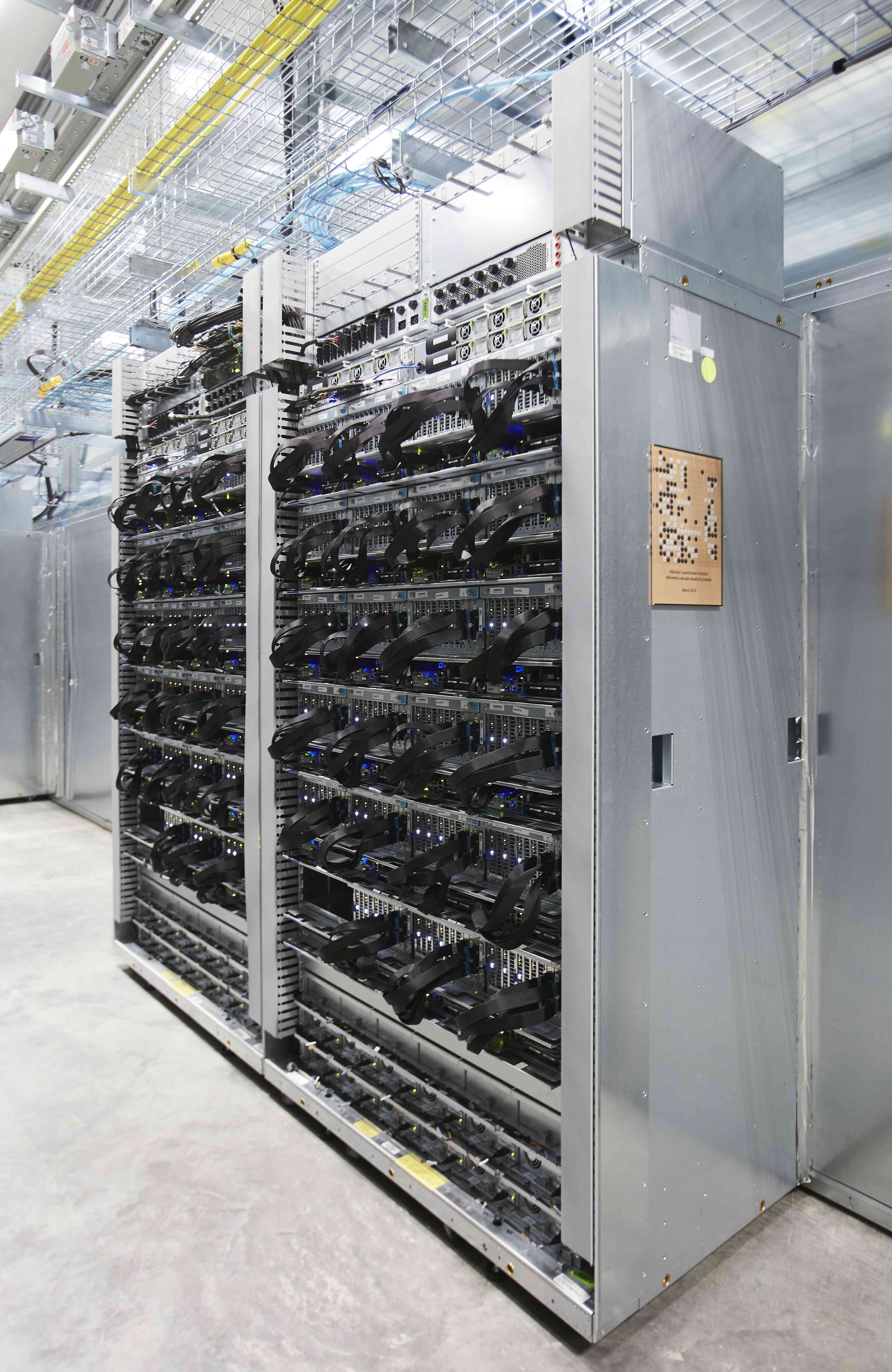
Norman P. Jouppi, a Distinguished Hardware Engineer at Google, declined to say if it was using TPUs for learning or for execution, but based on the use cases it cited, it is clearly using it to execute its machine learning algorithms. Jouppi says it is using the TPUs for Street View and Inbox Smart Reply, a feature that analyzes your email and offers three choices of response generated by Google’s AI. It was also used in the Alpha Go demonstration
Most companies pursuing machine learning today are have turn to massive parallelization to deliver the performance they need. For example, Facebook is using Nvidia GPUs in the specially designed servers it built just for implementing machine learning. IBM is testing a brain computing concept for eventual use, but in the meantime it is using an implementation of its Power architecture, CPUs and GPUs from Nvidia to run its cognitive computing efforts on.
 Nervana Systems, a company building a cloud-based AI service has adapted the firmware on Nvidia GPUs to deliver faster performance (its power consumption is unknown).
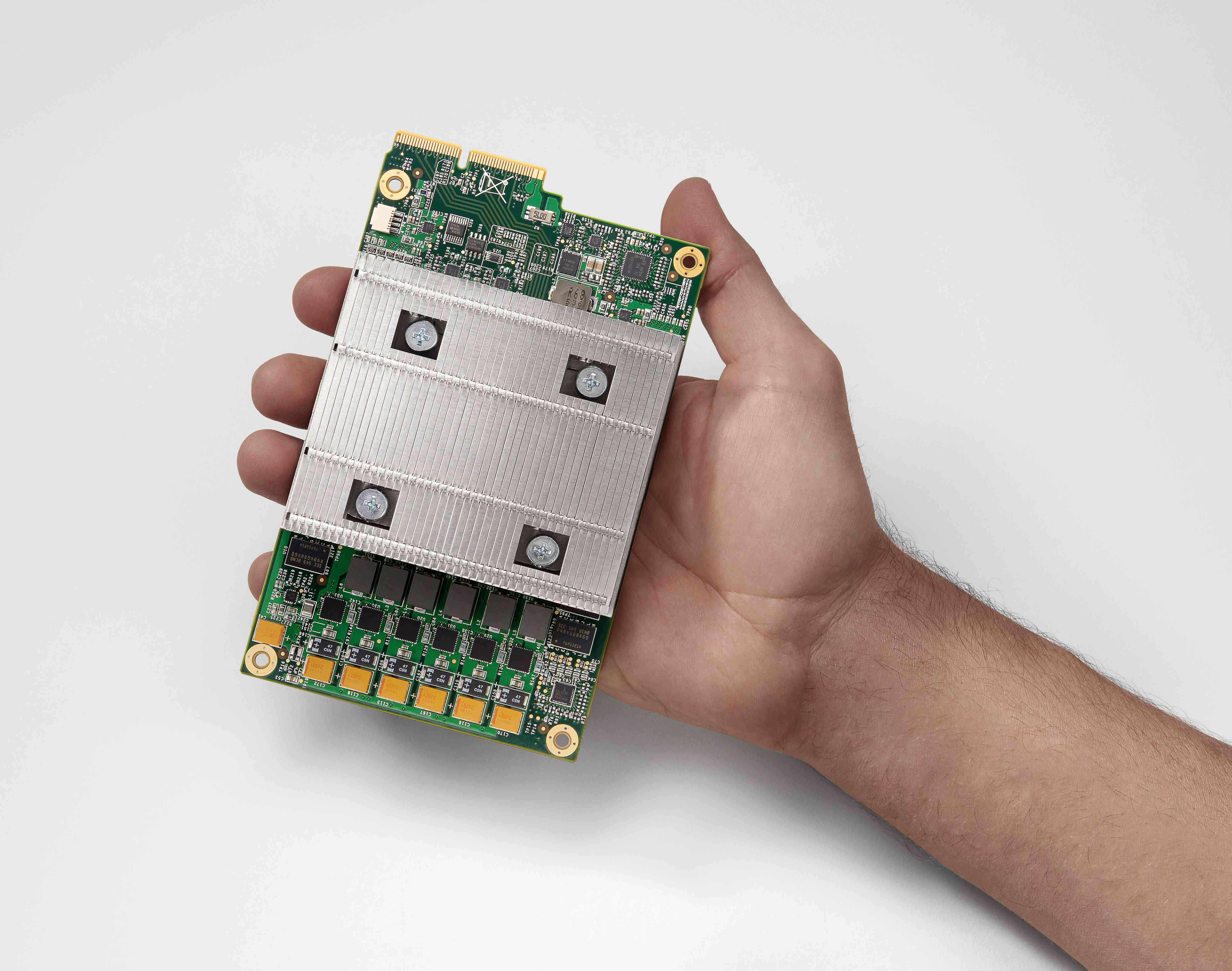
With its TPU Google has seemingly focused on delivering the data really quickly by cutting down on precision. Specifically, it doesn’t rely on floating point precision like a GPU does. Jouppi says that the focus on less precision meant it wasn’t using floating point math.
Instead the chip uses integer math, which Google’s VP for Technical Infrastructure Urs Hölzle confirmed for reporters in a press conference. At the time, Hölzle noted the TPU used 8-bit integer. Essentially this means that instead of wasting processing cycles worried about calculating things out to the umpteenth decimal point, the TPU can let a few slide, which means larger models can be used because of the lower resolution of the data.
This lack of precision is a common tactic for building out neural networks, where accepting probabilities in gigantic data sets tends to generate the right answer enough of the time. But it’s also not incredibly complex from a design perspective.
“Integer math isn’t something new,” says Kevin Krewell an analyst with Tirias Research. He is also skeptical about the power savings claims when compared with today’s graphics chips. Joupi said the TPUs have been in use for at least a year at Google, which means that these processors are best compared not to today’s machine learning chips, but to those built a year ago.
Google didn’t disclose what manufacturing node the TPU is built at, but it’s most likely a 28-nanometer node, which was the standard for a new GPU last year. Now the new Pascal chips from Nvidia are manufactured using a FInFET process at 16 nanometers, which wasn’t available a year ago.
Still, for a company like Google, the value of saving money for a year running it’s massive machine learning operations may have outweighed the cost of designing its own chips. Jouppi says that these are not processors that Google expects to be obsolete in a year. He also added that the focus wasn’t on the number of transistors, which suggests that a focus on moving down the process node to cram more transistors on a chip isn’t as important with this design.
As for the design, Jouppi explained that the decision to do an ASIC as opposed to a customizable FPGA was dictated by the economics.
“We thought about doing an FPGA, but because they are programmable and not that power efficient–remember we are getting an order of magnitude more performance per watt — we decided it was not that big a step up to customization.”
Krewell points out that designing a chip from scratch, even a simple one, can cost $100 million or more. So for Google the question is whether the time to market advantage on more efficient machine learning inference justifies and will continue to justify that cost. Without knowing what node Google is manufacturing at, the size of its operations (when asked what percent of machine learning workloads were running on TPUs, Jouppi said, “I don’t know.”) or the details of the chip itself, it’s hard to say.
Our bet is that is exactly how Google wants it. Remember this? The company has gained a considerable advantage by investing in its infrastructure–from buildings it’s own gear to building actual fiber connections. But with machine learning being the new bedrock for product innovation and delivering services, Google now has to adapt its infrastructure strategy to the new era.
Unfortunately its competitors have learned from Google’s previous investments in infrastructure, so they are hot on its heels, seeking the same efficiencies. And since Google rarely shares anything it doesn’t have to about its infrastructure until it had already squeezed the economic and technical advantage out of them, the TPU announcement feels a lot like marketing.
Jouppi says the company has no plans to open source it’s TPU design or license it, and he didn’t say when the company might release more details, although it sounded like Google would eventually release them. Maybe it is waiting for the completion of a newer, better design.
 Stacey Higginbotham has spent the last fifteen years covering technology and finance for a diverse range of publications, including Fortune, Gigaom, BusinessWeek, The Deal, and The Bond Buyer. She is currently the host of The Internet of Things Podcastevery week and writes the Stacey Knows Things newsletter all about the internet of things.
In addition to covering momentum in the Internet of Things space, Stacey also focuses on semiconductors, and artificial intelligence.


I agree, this is marketing. only an order of magnitude using a custom ASIC and reducing precition? Go to microarchotecture conferences and you will see much more benefits. I guess that they realized that this was not a big deal anymore so they try to get the hype… IBM did the TrueNorth chip quite before and I’m sure their implementation is much better
Actually no the TrueNorth chip isn’t doing so hot especially not on CNN which is what most hyperscaler use nowadays as it is good for Image/Video classification. That can drive a higher layer reinforcment learning. I think google is going the right way and this is obviously extremely bad news for the likes of nVidia who basically bet all their eggs currently on DL but their chips are way too power hungry to be even close to compete with a true optimized ASIC or even an synthesized FPGA.
Reducing precision for unstructured data sort dramatically improves system throughput to identify meta tables on which learning happens.
Noteworthy influencing decision making of heterogeneous compute platform architects is SIMD (single instruction multiple data) algorithms still tied to their traditional control plane processors.
The flip side is control side incumbent mass and processing plane leading advantage, tools, and the incredible long time forward thinking university education system churning out CUDA programmers.
There are learning system processing alternatives and platform architectures that eliminate the SIMD control plane legacy.
On Google development who’s licensing the core and basic IP blocks Google system logic is wrapped around? Because this is the new revolution.
Mike Bruzzone, Camp Marketing
The numerical solution of the ML problem is an iterative one of reducing the residual to zero. Precision is unimportant for most of the problem. The logistic function turns it into a nonlinear problem but it’s compensation is that it automatically scales numbers back to between +/- 1. Hence making it easier to work with integers (8-bits?).
There would be spectacular gains if they could also implement a digital logistic function. If the chip also has the ability to perform like a 32 bit GPU, the logistic function would be available .
I had thought that, since you are calculating gradients between -1 and +1 that you need minimal floating point, usually 16 bit half-floats. Are you certain they are doing Integer Math? If so, they you are probably right; this is an inference engine not a training engine.