There are lots of ways that we might build out the memory capacity and memory bandwidth of compute engines to drive AI and HPC workloads better than we have been able to do thus far. But, as we were reminded in a webinar we recently hosted with experts from Microsoft Azure, AMD, Cerebras Systems, and Ayar Labs, anything we might do – and there are many intriguing optical I/O options on the table – to have a new memory approach has to be manufacturable and cost-effective at scale.
Otherwise, it will not be – and cannot be – adopted.
Which is how we got the HBM bottleneck that we now have. A small percentage of very expensive HPC and then AI workloads that were bound on memory bandwidth had stacks of massively parallel HBM memory placed very close to the compute engines. HBM does nothing to help with memory capacity and memory bandwidth at the same time – you can only have just one.
HBM memory is so much better than using regular DRAM and bests GDDR as well for compute engines where bandwidth is the issue, but even with Micron Technology joining the HBM party with SK Hynix and Samsung, the world can’t make enough of this stuff to meet the demand. And that, in turn, is causing scarcity for high-end compute engines (along with the interposer packaging that HBM necessitates), which in turn is bending the market in unnatural shapes and causing big inefficiencies and imbalances between raw compute and memory capacity and bandwidth on them.
We have discussed the problem at length in many articles, and we are not going through the litany again except to say that to our way of thinking, the GPUs and custom AI processors coming out now and in the near future could easily have 2X and possibly 3X to maybe even 4X the HBM memory capacity and bandwidth to balance out their huge amount of compute better. When doubling up the memory on the same GPU delivers nearly 2X the performance on AI workloads, the memory is the problem and maybe you don’t need a faster GPU as much as you need more memory to keep it fed.
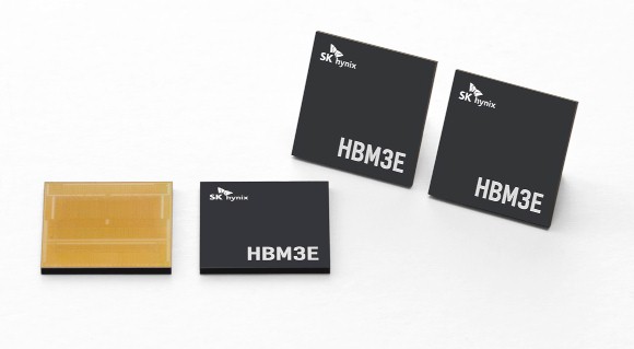
It was with this in mind that we considered two recent announcements from SK Hynix, which is the volume leader in HBM shipments worldwide and a key supplier to both Nvidia and AMD for their datacenter compute engines. This week, Kwak Noh-Jung, chief executive officer at SK Hynix, was speaking at the SK AI Summit in Seoul, South Korea and showed off a forthcoming variant of the HBM3E memory, which has been ramping up to volume in various products for the past year. What is exciting about this HBM3E variant is that memory stacks that are 16 chips high. That is a stack of DRAM chips per bank that is twice as high as the current HBM3E stacks used in many devices, and with 24 Gbit memory chips delivers 48 GB per stack.
This is a big improvement in capacity over the eight-high stacks of HBM3 and HBM3E that topped out at 24 GB of capacity per stack using 16 Gbit memory chips and the twelve-high stacks using 24 Gbit memory chips that topped out at 36 GB of capacity.
Before you get too excited, the 16-high stacks are being sampled with HBM3E memory but Kwak said that the 16-high memory would “open up from the HBM4 generation” and that the taller stacks of HBM3E were being created “in a bid to secure technological stability” and would be sampling to customers early next year.
You can bet that Nvidia, AMD, and other accelerator makers want to add such technology to their roadmaps as soon as possible. We shall see what happens.
SK Hynix said it was using the same advanced mass reflow-molded underfill (MR-MUF) technology, which melts the bumps between DRAM chips and fills the spaces in between them with goo to connect them together in a way that better dissipates heat for the stacks of chips. MR-MUF has been the hallmark of the SK Hynix HBM designs since it was introduced with HBM2E in 2019. HBM1 memory in 2013 and HBM2 memory in 2016 used a technique called thermal compression with non-conductive film, or TC-NCF, which was also used by Samsung at the time and continues to be its stack glue of choice. And Samsung contends that TC-NCF hybrid bonding is necessary for 16-high stacks.
But Kawk said that SK Hynix was developing a hybrid bonding technique for 16-high HBM3E and HBM4 memory just in case the yields don’t work out on the taller stacks. Which tells us, in a sense, that SK Hynix is a little worried. And we would guess that it is a variant of the TC-NCF process that it had experience with for HBM1 and HBM2 memory way back when.
Kawk also dropped some performance tidbits, saying that the 16-high HBM3E stacks would deliver 18 percent improvement in AI training performance and 32 percent improvement for AI inference performance. (We have no idea what metrics were used for these claims.)
Planning A Trip Down Memory Lane With The HBM Roadmap
Given all of this, and the presentations given by SK Hynix at the OCP Summit a few weeks ago, we thought it was a good time to look at the roadmaps for HBM memory and the challenges that SK Hynix and its competitors face as they try to push this technology to the limits so compute engine makers can avoid using optical I/O to link HBM to motors as we have been doing for a decade.
There are a bunch of SK Hynix HBM roadmaps floating around out there, each with different stuff on it. Here’s one:
And here is another one:
Let’s review. HBM1 launched in 2014 and was ramped in small volumes in 2015, and presumably had pretty low yield because it was a very new technique for boosting main memory bandwidth for compute engines. The initial HBM1 memory from SK Hynix was based on 2 Gb memory chips, which were stacked four high with a capacity of 1 GB of memory with 128 GB/sec of bandwidth using 1 Gb/sec I/O channels.
HBM2 was trotted out in 2016 and went commercial in 2018, and here the wire speed of the devices was pushed up to 2.4 Gb/sec, a 2.4X increase over HBM1 and delivering 307 GB/sec of bandwidth per stack. HBM2 stacks were four DRAM chips high to start but were boosted to eight chip stacks. The DRAM chips used in HBM2 were 8 Gb in capacity, and therefore a four-high stack topped out at 4 GB and an eight-high stack was double that at 8 GB.
This was starting to be interesting, and got even more interesting when HBM2E was unveiled in 2020. DRAM chip density doubled to 16 Gbit, which doubled up the capacity to 8 GB for a four-high and 16 GB for an eight high tower of main memory. The wirespeed of the DRAM was boosted by 50 percent to 3.6 Gb/sec, pushing bandwidth up to 460 GB/sec per stack. With four stacks, now a device could have 1.8 TB/sec of aggregate memory bandwidth, which was a lot more than what a traditional CPU with four or six DDR4 channels could deliver.
With the unveiling of HBM3E in 2022, concurrent with the launch of the “Hopper” H100 GPU accelerators from Nvidia and the beginning of the commercial GenAI boom, everything went crazy. The speed of the wires linking the DRAM to the CPU or GPU was boosted by a factor of 1.8X to 6.4 Gb/sec, delivering 819 GB/sec of bandwidth per stack, and the stacks came in at a base eight-high with a twelve-high option using 16 Gbit DRAM. That worked out to 16 GB for an eight-high or 24 GB for a twelve-high stack. It is deeply unsatisfying that sixteen high stacks did not happen with HBM3. But each new reach in height is more than incrementally difficult.
And so here we are, today, with HBM3E:
HBM3E was introduced in May 2023 by SK Hynix, and the pin speed on the DRAM was boosted to 8 Gb/sec, a 25 percent increase over HBM3 memory, pushing it up to 1 TB/sec per stack. The DRAM chips for HBM3E were 24 Gbit, yielding a stack capacity of 24 GB for an eight high and 36 GB for a twelve high. Because of its faster 9.2 Gb/sec signaling rate, Micron Technology’s HBM3E was chosen for the Hopper H200 GPU accelerator (with 1.2 TB/sec per stack), while the slower SK Hynix chips were chosen for a second update of the H100s used in the Grace-Hopper superchips and the H100-NVL2 inference engines from Nvidia.
Younsoo Kim, leader for DRAM technology planning at SK Hynix, talked through the HBM roadmaps from the company and went over the specific challenges needed to move to HBM4 memory, which is still an evolving standard and which is expected to make its debut in the next-generation “Rubin” R100 and R200 GPUs from Nvidia in eight high stacks in 2026 and twelve high stacks in 2027 with the R300s.
The “Blackwell” B100 and B200 GPUs are expected to use eight-high stacks of HBM3E for a maximum capacity of 192 GB, and the “Blackwell Ultra” follow-on due next year, which may be called the B300 if the rumors are right, will use twelve high stacks of HBM3E for a maximum capacity of 288 GB. (Nvidia has been playing around with product names, so we hear.)
We have been guessing that 16 high stacks were coming for HBM4, and are pleasantly surprised that SK Hynix is actually building DRAM stacks that high for HBM3E for testing purposes. So long as the yield is not terrible, AI compute engines sure could use memory capacity and bandwidth boosts ahead of schedule.
There are a lot of issues before we can get there, as Kim explained in his OCP presentation, which you can see here. For one thing, the compute engine makers are pushing all three HBM memory makers to boost bandwidth higher than the initial specs they agree to, while at the same time asking for lower power consumption:
We want a little red wagon, a sailboat, a puppy, and a pony for Christmas, too, but just because you put something on a list doesn’t mean you will get it.
The need for lower power is made all that more difficult as compute engine makers are taking the hood off their devices and letting them get hotter faster than the performance increases to get incremental performance. That is how we went from 240 watts with a “Kepler” K40 GPU accelerator from Nvidia in late 2013 to an expected 1,200 watts for the full-bore Blackwell B200 accelerator. The B100 and B200 are comprised of two Blackwell chiplets, each with four HBM3E stacks, for a total of eight stacks that are eight memory chips high. That 192 GB of memory provides a combined 8 TB/sec of bandwidth. We can remember when entire supercomputer clusters with thousands of nodes had a staggering 8 TB/sec of aggregate memory bandwidth.
By the way, we think that bandwidth can be pushed up to 9.6 TB/sec using Micron HBM3E memory in the B300, should that come to pass.
It is a pity that HBM4 memory density is not increasing in 2026 as the memory stacks are also growing to sixteen high. Perhaps the memory makers will surprise us with fatter HBM4E memory that comes in at 32 Gbit instead of sticking with the 24 Gbit chips that this chart from Kim’s presentation shows:
The handling of the thin wafers used in HBM memory is a concern for yielding, as is the MR-MUF process for gluing the DRAM together into stacks. (More on that in a second.)
Thermal issues are a challenge, too. Memory is very sensitive to heat, especially if you have a bunch of it pancaked up like a skyscraper next to a big, fat, hot GPU compute engine that has to be less than 2 millimeters away from that memory so the signaling works right.
So those are the challenges to advancing HBM memory for compute engines. What can SK Hynix do about all of this? Do what we always do: Make stuff wider and couple them together better.
HBM3E has a 1,024-bit wide channel, and HBM4 will double that to 2,048 bits. It looks like both 24 Gbit and 32 Gbit DRAM chips will be supported with HBM4 (possibly with the latter being used for HBM4E, but we are not sure.) A sixteen high stack with 32 Gbit chips would yield 64 GB of memory per stack, which would be 256 GB for each Nvidia chiplet on a Blackwell package, or 512 GB per socket. If Rubin stayed at two chiplets and was just an architectural enhancement, that would be cool. But Rubin might be three GPUs interconnected or even four, with HBM running down the sides.
Imagine an Nvidia R300 package with four GPUs, and sixteen stacks of sixteen high 32 Gbit memory, for a total of 1 TB per compute engine. Put some RISC-V cores on that for running Linux, add NVLink ports and a UEC Ethernet port running at 1.6 Tb/sec and call it a server and be done with it. . . .
In addition to the wider buses, Kim suggested that integrating the memory addressing logic in the base die of the HBM stack, rather than in a separate chiplet in the interposer of in the HBM controller, was also a possibility, lowering the power needed to do memory control across the link between compute and memory.
This approach would also allow for the complete testing of an HBM stack separate from the finished AI compute engine. You could get known good stacked dies and weld them onto the compute engine socket after you know that, not before.
When all is said and done, HBM4 is expected to offer more than 1.4X the bandwidth, 1.3X the capacity per memory chip, 1.3X the capacity from a higher stack (sixteen versus twelve, not shown in the chart below because it is probably going to be saved for HBM4E unless Nvidia and AMD can talk SK Hynix out of it and the yields are good enough to not lose a fortune using the cutting edge denser and faster memory), and burning only 70 percent of the power of HBM3/HBM3E.
While this is all well and good, what seems apparent to us is that we need such memory as promised for 2026 and 2027 right now. Because of the memory-compute imbalance, customers are spending a fortune on a device that cannot come close to its peak performance because of bandwidth and capacity bottlenecks in the HBM memory. We either need HBM4E memory early, or as we wrote about back in March this year when covering the simultaneous bi-directional NuLink PHYs from Eliyan, we need a way to hook a lot more HBM3E memory to the current devices.
Better still, let’s double up the number of stacks and also get HBM4E now for Nvidia Blackwell and AMD Antares GPUs.
Notice we didn’t ask for 24 high stacks. . . . That would be greedy.


So if a remake of the The Graduate was filmed in 2024, “the word” would be “HBM”? // instead of “plastics”
OK, you made me laugh, Carl.
Hmmmm, sounds like a spectacular battle royale might be brewing here between the liquid Mr. MUF’s rulebreaker spirirt and the solid Mr. DIMM’s mineralogical ethos, for the ultimate championship crown of the “tearing down that memory wall” extravaganza!
Will Mr. MUF’s advanced mass reflow-molded underfill suplex be the secret sauce that beats Mr. DIMM’s multiplexed rank top-rope dual-sledge inline polish-hammer modules? Will Mr. MUF’s 40% thinner stature successfully resist chip warpage in 12- and 16-high giant sandwich stacking pyramid skyscrapers of the intended Human Bodily Mashup (HBM)? Will the gap-filling Epoxy Molding Compound (EMC) efficiently evacuate all needed heat, sweat and gore from the pugilist pile to fully enable 2,048 bit reverse wheelbarrow action?
The excitment is palpable, with answers to be provided only in the ring! Let the memory wall Rhumbamageddon begin! 8^b
Netlist is working with SK Hynix on that issue.