

If Nvidia and AMD are licking their lips thinking about all of the GPUs they can sell to the hyperscalers and cloud builders to support their huge aspirations in generative AI – particularly when it comes to the OpenAI GPT large language model that is the centerpiece of all of the company’s future software and services – they had better think again.
We have been saying from the beginning of this generative AI explosion that if inference requires the same hardware to run as the training, then it cannot be productized. No one, not even the deep-pocketed hyperscalers and cloud builders, can afford this.
Which is why researchers at the University of Washington and the University of Sydney have cooked up a little something called the Chiplet Cloud, which in theory at least looks like it can beat the pants off an Nvidia “Ampere” A100 GPU (and to a lesser extent a “Hopper” H100 GPU) and a Google TPUv4 accelerator running OpenAI’s GPT-3 175B and Google’s PaLM 540B model when it comes to inference.
The Chiplet Cloud architecture was just divulged in a paper based on research spearheaded by professors Michael Taylor, of the University of Washington, and Shuaiwen Leon Song, of the University of Sydney who also happens to be a visiting professor at the University of Washington and has just joined Microsoft earlier this year.
Interestingly, Song was a senior staff scientist and technical lead at Pacific Northwest National Laboratory as well as a faculty member working on future system architectures at those two universities before joining Microsoft in January of this year as senior principle scientist to co-manage its Brainwave FPGA deep learning team and to run its DeepSpeed deep learning optimizations for the PyTorch framework, which are both part of Microsoft Research’s AI at Scale collection of projects. On the original paper, Song’s Microsoft email was listed and we assumed this was the affiliation for the Chiplet Cloud research, as is commonly done in papers. But this was in error, and Taylor and Song both sent us a note saying this research predates Song’s Microsoft jobs and has no affiliation with Microsoft.
That said, we think Microsoft had better look at what Taylor, Song, and their co-researchers are proposing. Because it is interesting.
(An aside: Not for nothing – and we really mean that as you will see – the projects that Song is taking over are among the projects that were bested by GPT, forcing Microsoft to shell out a $10 billion investment in OpenAI at about the same time Song was joining Microsoft. To date, Microsoft has given OpenAI $13 billion in investments, much of which will be spent to train and run GPT models on Microsoft’s Azure cloud.)
A Massive Array Of Matrix Math
If we had to summarize the Chiplet Cloud architecture in one sentence, which we kinda have to do, it would be this: Take a wafer-scale, massively parallel, SRAM-laden matrix math engine like the one designed by Cerebras Systems, hold it in the air perfectly level, and let it drop on the floor in front of you and then pick up the perfect little rectangles and stitch them all back together into a system. Or rather more precisely, instead of doing waferscale matrix math units with SRAM, make a whole lot of little ones that have a very low individual cost and a very high yield (which also pushes that cost down), and then stitch them back together using very fast interconnects.
The approach is akin to the difference between what IBM was doing with its BlueGene line of massively parallel systems, like the BlueGene/Q installed at Lawrence Livermore National Laboratory, and what it did with the GPU-heavy iron in the “Summit” supercomputer at Oak Ridge National Laboratory. BlueGene, very much like the “K” and “Fugaku” systems at RIKEN Lab in Japan, in the long run might have always been the right approach, only we would need different processors tuned for AI training and HPC calculations and for AI inference.
We have been talking about the enormous cost of building systems to run transformer-based generative AI models in recent weeks, and the Chiplet Cloud paper does a nice job of laying out why Amazon Web Services, Meta Platforms, and Google have been trying to find ways to make their own chips to make AI inference less expensive. Microsoft is no doubt thinking along the same lines.
“Serving generative transformer-based large language models on commodity hardware, like GPUs, is already hitting a scalability wall,” the researchers, who include Huwan Peng, Scott Davidson, and Richard Shi at the University of Washington, wrote. “State-of-the-art GPT-3 throughput on GPU is 18 tokens/sec per A100. ChatGPT and the promise of integrating large language models into various existing technologies (e.g. web-search) puts into question the scalability and profitability of large-language models. For example, Google Searching processes over 99,000 queries per second. If GPT-3 is embedded in every query, and assuming each query generates 500 tokens, Google needs 340,750 Nvidia DGX servers (2,726,000 A100 GPUs) to keep up. The cost of these GPUs exceeds $40 billion in capital expenditure alone. Energy consumption will also be huge. Assuming a 50 percent utilization, the average power would be over 1 Gigawatt, which is enough energy to power 750,000 homes.”
The problem with the GPU – any GPU, not just those created by Nvidia – is that they are general purpose devices and therefore they have to have a lot of different kinds of compute to satisfy all of their use cases. You know this is true because if it wasn’t, Nvidia GPUs would just have Tensor Core processors and not vector engines as well. And even with a device like Google’s TPU, which is essentially just a Tensor Core processor, the size and complexity of the device, with its HBM memory stacks, makes it very expensive to deliver even if it does, at least according to the comparisons in the paper, offer much better total cost of ownership (TCO) than an Nvidia A100 GPU. Like this:
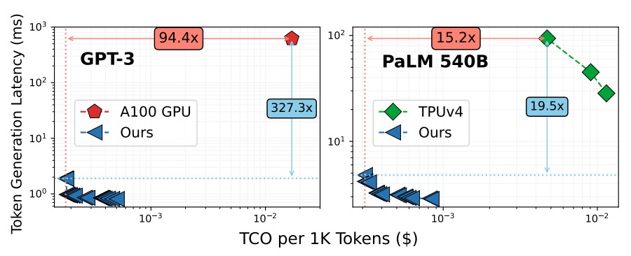
Note: This Chiplet Cloud paper gets pricing for A100 capacity on the Lambda GPU Cloud and TPUv4 pricing comes from the Google Cloud, of course.
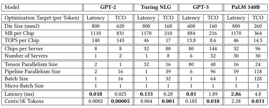
And here is the data underlying the chosen reference data points in the chart above, which is fascinating:
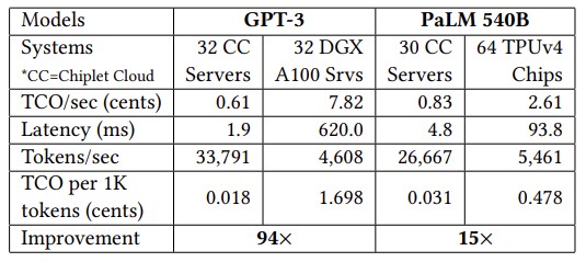
On the GPT-3 model with 175 billion parameters, the simulated Chiplet Cloud devices had a stunning 94.4X reduction in cost per 1,000 tokens processed for the inference and an absolutely amazing 327.3X reduction in token generation latency compared to Nvidia’s A100 GPU. Even if the throughput of the H100 is 3.2X higher than on the A100 (which is comparing INT8 throughput on the A100 to FP8 throughout on the H100), we have no reason to believe the latency will be that much different even with HBM3 memory that us 50 percent faster. And even if it was, the H100 costs about 2X on the street what an A100 costs right now. The H100 would be down and to the left of the A100 on the chart above, to be sure, but it has a very big gap to close.
The shift to a tensor core style matrix math engine with HBM memory helps to a certain extent, as the right side of the chart above featuring the TPUv4 compute engine shows, and even with a much larger PaLM model with 540 billion parameters. The theoretical Chiplet Cloud shows a 15.2X reduction in cost per 1,000 tokens generated running inference and a 19.5X reduction in latency.
In both cases, the Chiplet Cloud is optimizing for low cost per token and paying for it with a reasonable amount of latency. And clearly with the Chiplet Cloud architecture it can drive down latency a little bit lower if customers are willing to pay a proportionately larger higher cost for those inferrings.
We love this chart, which shows why the hyperscalers and cloud builders are thinking about custom ASICs for AI inference, particularly when LLMs need so much compute and memory bandwidth to do inference:
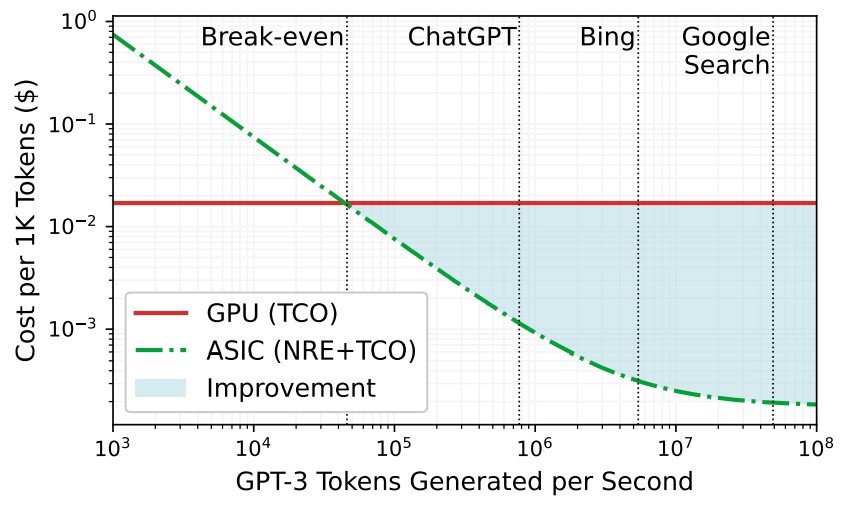
The denser the AI work, the better the cost improvement is for using an ASIC compare to using a GPU, and incidentally, this chart also suggests Google search is much more intensive than Bing search and lower cost, too. (Hmmmmm. . . . Don’t count Bard out just yet.) The breakeven point between the GPU and the custom ASIC is at around 46,000 tokens per second. This performance was based on Microsoft’s own DeepSpeed-Inference engine running on the Lambda GPU Cloud at a cost of $1.10 per hour per GPU against a DeepSpeed-Inference run on a simulated Chiplet Cloud accelerator.
In designing its Chiplet Cloud, the researchers came to a few conclusions.
First, the cost of producing the chip is a big part of the overall TCO of any computing engine.
By our estimates, GPUs represent 98 percent of the compute capacity and probably 75 percent of the cost of a modern HPC/AI supercomputer. They reckons that the cost of making an accelerator for LLM inference is around $35 million for a chip etched in a 7 nanometer process, which includes the cost of CAD tools, IP licensing, masks, BGA packaging, server designs, and human labor. Against a potential $40 billion investment, this is peanuts. This is peanut dust.
This means you can’t use reticle-busting compute engines if you want to drive down costs. The researchers said in the paper that for 7 nanometer processes from Taiwan Semiconductor Manufacturing Co, with a defect density of 0.1 per cm2, the unit price of a 750 mm2 chip is twice that of a 150 mm2 chip.
Second, inference is as much a memory bandwidth problem as it is a computational one.
To make the point, unfortunately using an older GPT-2 model and an equally older Nvidia “Volta” V100 GPU, most of the GPT-2 kernels had low operational intensity – meaning they didn’t need much flops after all – and were limited by the 900 GB/sec of HBM2 bandwidth. Moreover, the researchers calculated that it would take 85,000 GB/sec – nearly two orders of magnitude more bandwidth – to drive the entire 112 teraflops of computing oomph in the V100 GPU to run GPT-2 efficiently.
And given this, the secret to the Chiplet Cloud is exactly what Cerebras Systems, GraphCore, and SambaNova Systems already figured out: Get the model parameters and their key value intermediate processing results that are recycled to speed up generative models all into SRAM as close to the matrix math engines as possible. The gap is huge here between DRAM and HBM:
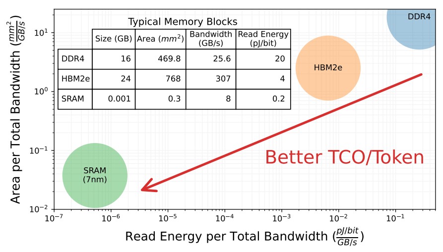
So SRAM seems to be a no brainer here.
The other thing is that there needs to be a way to mitigate package costs for chiplet designs as well as limiting inter-chip communication, which increases the inference latency and decreases throughput. So the researchers are proposing the use of a chiplet as a package and doing the integration at the board level, not the socket level, and is using tensor and pipeline parallelism mapping strategies to cut down on inter-node communication across the Chiplet Cloud boards. And each chiplet has enough SRAM to hold the model parameters and KV cache for all computational units. In effect, you have a massively distributed cache that is then chewed on by individual chiplets as they do their own unique inferences.
The proposed Chiplet Cloud looks like this:
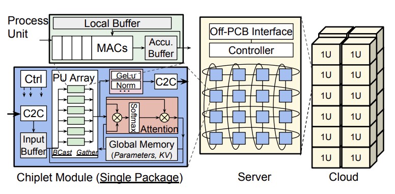
And it has no silicon interposer or organic substrate integration that adds to cost and complexity and that lowers package-level yield, which is also an issue with these big, fat, wonderful devices like GPUs and TPUs. The chiplet board connects a bunch of chiplets in a 2D torus using printed circuits, which the researchers say is flexible enough to accommodate different mappings of the devices. (This is similar to what Meta Platforms was doing on the circuit boards for its GPU accelerator systems using PCI-Express switching as an interconnect.) The circuit board has an FPGA controller, and each chiplet has a full-duplex link running at 25 GB/sec with 80 mm reach using ground reference signaling. Other kinds of interconnects could link the nodes together as needed, they say.
They add that different models would require different chiplet compute and memory capacities for different models and for whether they are optimized for latency or TCO. Which is very interesting indeed:
The lesson here is that one size never fits all. You can have something that is more general purpose, but you always pay with lower efficiency. Cloud builders need general devices because they never know what people will run – unless they just intend to sell services against a proprietary software stack, in which case they can optimize like crazy and give the best price/performance and keep some of the leftover money – which only happens if they don’t over-optimize – as profits.
Wouldn’t it be funny if Chiplet Clouds were manufactured and sold to Google that were optimized to run PaLM 540B? Or stole TPU customers away from Google Cloud to Microsoft Azure if it manufactured a custom Chiplet Cloud geared to PaLM 540B? Stranger things have happened. And the idea is out there now, and it can be a bargaining chip against Nvidia and AMD. Some of you who have always wanted a startup might be able to use this idea to create a clone of what the researchers have suggested. Groq did that with the TPU, and AI venture capital seems to be still relatively freely available. Why not?

With ROCm Software And Instinct MI200 GPUs, AMD Has Ecosystem Critical Mass
Paid Feature Great hardware is the foundation of any compute platform. But hardware, in and of itself, is never sufficient to create a platform. And in fact, it takes two other important things for any platform to be realized. After the hardware, a platform requires a complete stack of software …
What Chip Startups Can Learn from Google’s TPU Design Team
The inception of Google’s effort to build its own AI chips is quite well known by now but in the interests of review, we’ll note that as early 2013 the company envisioned machine learning could consume the majority of its compute time. Inference was a particularly expensive proposition, forcing Google …

Future Proofing Inference Servers With PCI-Express Switches
At this point in the history of datacenter systems, there can be no higher praise than to be chosen by Nvidia as a component supplier for its AI systems. Which is why upstart interconnect chip maker Astera Labs, which is taking on the likes of Broadcom and Marvell for PCI-Express …
If the key takeaway is to get KV cache and other parameters in memory as close to the matrix multiplication engines as possible, isn’t a perfect opportunity to leverage an FPGA architecture? Would a build-out of FPGAs be more or less than the $35M estimated for an ASIC?
An ASIC burns less juice than an FPGA. And you gotta figure, with all that Brainwave experience, Microsoft would use an FPGA if the price and performance made sense. I wonder what the biggest, fattest FPGA costs these days?
ASICs are way less costly, way faster and much cheaper in quantity. You pay in turn around time and debugging effort. I’ve worked at places where the original product went out in FPGA so they could do updates as needed. Once it was stable, they did a cost reduction ASIC spin to save money. Didn’t lower the price of the hardware… but kept more money.
I would assume in this case going straight to ASIC is the way to go, especially since they’re logically fairly simple designs, they just want close memory, connectivity, and a bunch of matrix engines. Once they debug it in FPGAs… they cost reduce like crazy since the payout is super quick. It’s just three to six months from sending the design files to TSMC before you get hardware back…. that’s the only reason they’d do this on FPGAs first.
Great article! If I understand, Chiplet Cloud means chips with very large amounts of SRAM (200MB to 1.2GB in their Table 2) and very long pipelines (16 to 118 stages in their Figure 11) resulting in best TCO and throughput for serving LLM-type workloads (especially the multiple Fully-Connected (FC) Feed-Forward decoder layers, in their Fig. 2). To be frank, these look to me like “way-out” design points (eg. face-down hybrid-bonded 3D V-cache is just 64MB of shared L3, x86 pipelines have maybe 14 stages?) — but if it works and saves energy and money … (and suddenly makes H100s and MI300s less expensive for the rest of us …) then Yes! Go forth and matrix multiply!
OK, HuMo, you win! Go forth and matrix multiply indeed!
HBM memory is making huge progress, see HBM3e and next gen HBM4 specs, they can do up to 6 TB/s and 10 TB/s when 6 to 8 stacks are put together. Not even mentioning the memory size advantage of HBM memory (80 GB for H100 and 192 GB for MI300). the only advantage left for SRAM is low latency. Next gen HBM should be faster (more bandwidth) than sram and sram is not easily scalable, hbm memory scales much better. Finally there is also processing in-memory HBM which resembles the solution you are describing in your article.
I think this goes back to the 85 TB/s figure in the “unfortunately using …” paragraph of this TNP article, which refers back to Figure 4 in the Chiplet paper. For HBM4 at 10 TB/s, the V100 would still need to perform 10-20 flops-of-processing/byte-of-accessed-mem for fullish utilization of the GPU’s oomph — if I correctly mis-exfoliate … (100 flop/byte at 0.9 TB/s on the fig.)
It could be that emerging Non-Volatile Memory (NVM) MRAM, like the VG-SOT-MRAM from European research center IMEC could help increase the cache density (replacing part or all the SRAM cache) AND also improve power efficiency as it is Non-Volatile (load the parameters in the cache once, and they stay there without needing energy to retain the information: it is a bit like bi-stable E-ink).
It’s a wonderful concept but the devil is in the details. You referenced Cerebras Systems in the piece, take a look at SeaMirco and ask why did the same core engineers go with wafer scale.
Thanks for the analysis on the article!
Please note that this work was led by the University of Washington, and Dr. Song’s contributions predate his joining Microsoft.
Michael Taylor
Professor
U. Washington
This article was written when I was in the university. It has nothing to do with Microsoft. We were professors writing an academic paper. We made a mistake about the affiliation and now we are updating a newer version reflecting my previous university affiliation. Could you please take this article down or modify it to talk about this research work done by university of Washington team. Thank you very much.
There is other low hanging LLM fruit ASICs can pick, like chunked 3-8 bit quantization modern GPUs aren’t really designed for, or optimization for specific software attention schemes.
If I am multiplying it right, 175B GPT-3 minimum latency calls for 414GB of SRAM. That doesn’t sound like ~4 bit quantization to me.
So what is the difference (architecturally) between this Chiplet Cloud and the Tesla Dojo that was presented at the last Hot Chips?
Dojo is using pretty advanced packaging. Similar in concept, for sure, with precise interconnects.
Two things come to mind:
– Wouldn’t it be wonderful if demand for GPUs from big tech dropped off like it has from crypto miners? Normal people could buy decent GPUs again.
– Google search vs Bing search number of ops needed: since Bing is so much more an advertizing engine this makes sense. Serving paid results would involve more simple hash lookups and less inference.
I fully expect that to happen at some point, but heaven only knows when. This Dot Cog Boom will probably not take as long as the Dot Com one did. We are a lot faster at the hype cycle these days, eh?
The memory limitation problem dogging the immortal computing paradigm is correctly identified by the paper and to some extent this article. Already the HBM in an H100 costs more to manufacture then the GPU die itself, and it (the memory) is still too slow and too small. At the same time though, its far too early to invest in fixed function ASICs optimised specifically for these transformer workloads. The mooted TCO gains would only ever materialize if the algorithms fail to advance meaningfully in the next 5-10 years which is not a likely outcome. That said the points made in the article and paper about the real world economics of LLMs are quite correct.
Sram scaling is dead after 3nm so not sure that the idea that the way forward is to expand SRAM to fit these huge models inside is the right one. This is where Graphcore started; either they were early, or wrong. A related point on sram scaling is that the compute becomes ever cheaper and thus ever more irrelevant in $ and mm2 versus the memory. So why prematurely optimise to an extremely fixed function compute solution, surely better to have something more general purpose (but not GPU sized)? The SRAM can always be stacked vertically to make room for that.
The parameter count is still vast versus the size of the training set. The algorithms for training and the model structure and assumptions themselves need to be fixed to deal with this fundamental flaw before genAI for all becomes economic; a very fixed function ASIC-write-large doesn’t alter the situation. I expect more innovations to follow before long that should improve efficiencies from the top down. Attention is seemingly, *not* all that is needed.
Well said. Thanks.