
It seems like we have been talking about Google’s TPUv4 machine learning accelerators for a long time, and that is because we have been. And today, at the Google Cloud Next 2022 conference, the search engine, advertising, video streaming, enterprise application, and cloud computing giant will finally make its fourth generation – and most powerful and scalable – Tensor Processing Units available to the masses.
Google has been trickling out information about the TPUv4 architecture for several years without being terribly specific about the feeds and speeds of the system. But we talked to some of the people behind the TPU effort and also poured over research papers and technical presentations to bring it all together to put together an overview of the four generations of TPU compute engines and the systems that make use of them. Where we could not find out information, we made what we reckon are intelligent guesses as is our habit.
There’s a lot to go over, so let’s get started.
It is perhaps important to remind everyone why Google decided to do custom silicon for AI training and inference in the first place. Back in 2013, as Google was working on voice activated search capabilities for its eponymous search engine, Jeff Dean, the Google Fellow who has had a hand in so many of its key technologies it is hard to list them all here, did a little bit of math on a piece of scrap paper and figured out that if this AI-assisted search went into production then Google would have to double its datacenter footprint. This, of course, is not feasible for a product that is “free.” There was not suddenly going to be 2X more search advertisers to support such an expansion. And so, Google got to work to build a better math engine for AI training and inference.
Without further ado and fuss, here are the relevant feeds, speeds, scales, and costs of the four generations of TPU iron, including a TPUv4i sub-variant that we had not realized was created until we ran across this paper by Norman Jouppi and a slew of other people (including Google Fellow David Patterson).
The TPU is an example of a domain specific architecture in action, and we think it is significant that Google has followed the trail of Nvidia in that it has created a general purpose motor that can do both training and inference, and at the same time it also has created a subvariant that is tuned specifically for inference – and in the case of the TPUv4i, tuned for its own internal inference workloads, not one available for those who want to run inference jobs on the Google Cloud. At least not yet.
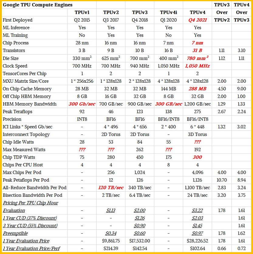
As it turns out, this TPUv4i inference chip went into production considerably ahead of the TPUv4 general purpose engine, which is backwards from the way Nvidia does it and which is also indicative of the fact that Google really, really needs cheap inference to drive the dozen or so applications that make use of its TPUs to add AI processing to augment their functions. Google has not been precise when it actually put the systems using the full TPUv4 into production, and we are guessing it is around Q4 2021.
Google has not been shy about stay back a node or two with its TPU designs, and that is absolutely on purpose to keep the cost of chip design and production low. A big portion of the cost of a leading edge compute engine comes from having bad yields on a leading edge process, and while you can mitigate that cost a bit by adding spare components to the design, that comes at a cost, too. By hanging back, the chip is cheaper on a number of vectors and also easier to get through the supply chain and into Google’s hands.
The TPUv4i inference chip was manufactured using Taiwan Semiconductor Manufacturing Co’s 7 nanometer processes and went into production a year and a half ago, and we think that the full-on TPUv4 is also using the same 7 nanometer process. We have been hemming and hawing about this in our prior coverage and put the gun to our head and that’s our final answer. We figure that 5 nanometer processes will be saved for TPUv5i and TPUv5 compute engines, which are almost certainly in testing if Google has TPUv4i and TPUv4 in production and the TPUv4 generally available to customers on the Google Cloud.
The basic structure of the TPU core is that it has a scalar and vector processor front end with a homegrown matrix math unit that does BF16 (a format invented by Google for its TPUs) multiply and FP32 accumulate operations (and sometimes INT8 for inference, depending on the model).
The original TPUv1 processor had a 256×256 matrix math unit, which is pretty hefty and, as Google learned along the way, not the optimal configuration. And, as it turns out, neither is a 64×64 array for Google’s own AI applications.
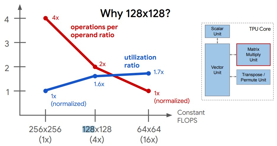
The sweet spot between matrix throughput and utilization is a 128×128 array at least for Google’s own code, and once Google figured that out, the company has increased the scale of the TPUs by either adding TPU cores (which have the MXU units embedded in them) or adding MXU units to each core, or by doing both at the same time.
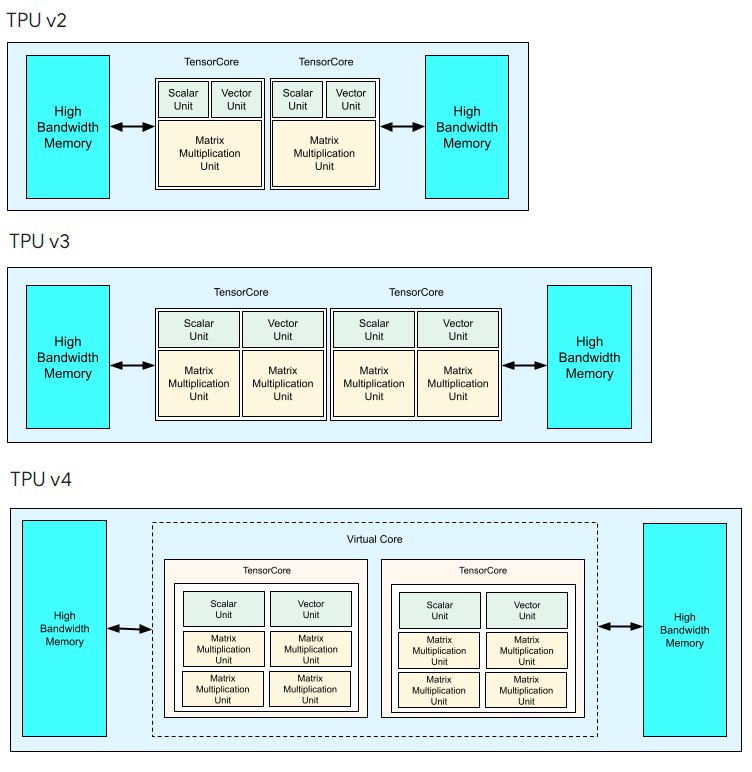
Here is the evolution of the designs from the TPUv2 through the TPUv4, which had the 128×128 array MXUs:
And just to complete the set, here are what the server boards using each generation of TPU look like on the outside:
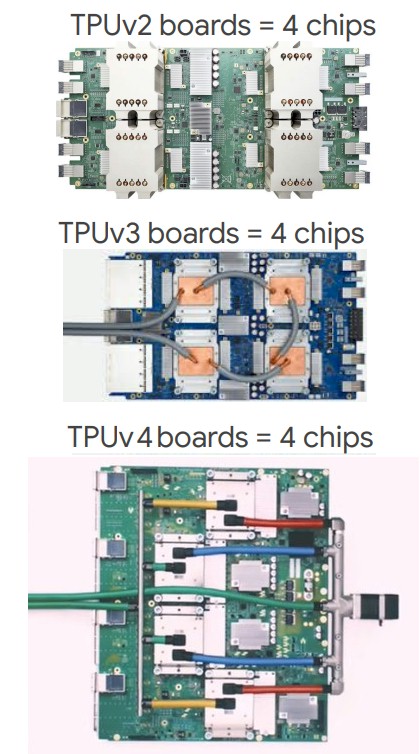
On the right of the TPUv4 server boards you see some adjacent chips. That is a six port switch acting as a network interface card and the foundation of a 3D torus network. From what we can tell, each port runs at 448 Gb/sec. Two of the ports implement a ring connecting four of the TPUv4 chips on the system board to each other, and four of them connect out to adjacent nodes in the 3D torus cube. If you do the math, the total bandwidth connecting hosts is 4 * 4 * 56 Gb/sec * 8, and then double it for both ways, which is about 7.12 tbps of raw bandwidth and 6 tbps of effective bandwidth. This compares quite well with a GPU server that has eight 200 Gb/sec InfiniBand ports that has 1.6 Tb/sec of aggregate bandwidth between hosts. (More on that in a bit.)
We were uncertain if Google would add cores or expand MXUs when we were talking about the TPUv4 chips, and as it turns out, it has kept the core count at two and once again doubled up the number of MXUs per core. And unless something changes, this is the way Google will create TPUv5, TPUv6, and so on. At some point, Google will go to four cores, we think, depending on what its homegrown XLA machine learning compiler can do, but at the moment, presenting a fewer number of cores is the easiest way to scale applications.
You will note that the TPUv4i inference chip is pretty hefty in its own right, with a single TPU core with four 128×128 MXUs, running at a very respectable 1.05 GHz but only taking up 400 mm2 of area. As far as we can tell, based on some floorplan estimates, doubling up the MXU count on a single core and doubling up the caches and goosing a few other uncore features to create the full-on TPUv4 with a single core might have only had boost the die size to around 563 mm2 or so.
But for whatever reason – probably having to do with optimizations for two-core TPUs in the XLA compiler – Google did a two-core TPUv4 AI training engine and we think it comes in at around 780 mm2 in area. From what we have seen, this two core TPUv4 chip presents itself as one logical core with a single 32 GB HBM memory space. We suspect it is a monolithic design, but it could be comprised of two of the TPUv4 chips lashed together in a single socket, which would lower costs but might impact performance depending on the in-socket interconnect Google might create or license. We highly suspect it is a monolithic design with logic blocks that were always meant to be doubled up.
All About The Scale
Let’s talk about scales on all of these different vectors in the past three core TPU generations for a second. The TPUv3 was an incremental “midlife kicker” upgrade over the TPUv2, with a 30-ish percent boost in a lot of the feeds and speeds and only a nominal 11 percent increase in transistor count and 12 percent increase in die size on the same process (16 nanometer) to yield a factor of 2.67X increase in chip performance with a 2X increase in HBM main memory capacity (letting it take on larger datasets). The big difference with the TPUv3, as far as we are concerned, is that the 2D torus interconnect was expanded from 256 chips in the TPUv2 chips to 1,024 chips in the TPUv3 generation, which resulting in the pod processing capacity increasing by 10.7X, from 12 petaflops to 126 petaflops (as measured in BF16 operations).
The TPUv4 is a real upgrade of the compute engine, with a process shrink from 16 nanometers to 7 nanometers and all of the goodness that allows. The number of MXUs is doubled up again, cache memory goes up by 9X to 244 MB (we think), HBM2 memory bandwidth goes up by 33 percent to 1.2 TB/sec but interestingly HBM2 memory capacity stays the same at 32 GB.
The reason Google can do that is that it can scale the TPUv4 pods like freaking crazy. Nvidia is bragging about how it can tightly couple up to 256 “Hopper” GH100 GPU accelerators with its NVSwitch fabric, but with the new 3D torus interconnect that debuts with the TPUv4, which has a lot more bandwidth and higher radix, it can tightly couple 4,096 TPUv4 engines together, for an aggregate of 1.126 exaflops of BF16 compute. (Eight of these TPUv4 pods are located in Google’s Mayes County, Oklahoma datacenter, yielding an aggregate of 9 exaflops of raw AI compute.)
Not a lot of AI workloads actually process across those 4,096 TPUv4 chips at the same time, which is why a 3D torus is useful. It allows for the machine to be sliced up into tightly coupled chunks that are still interconnected so they can share work.
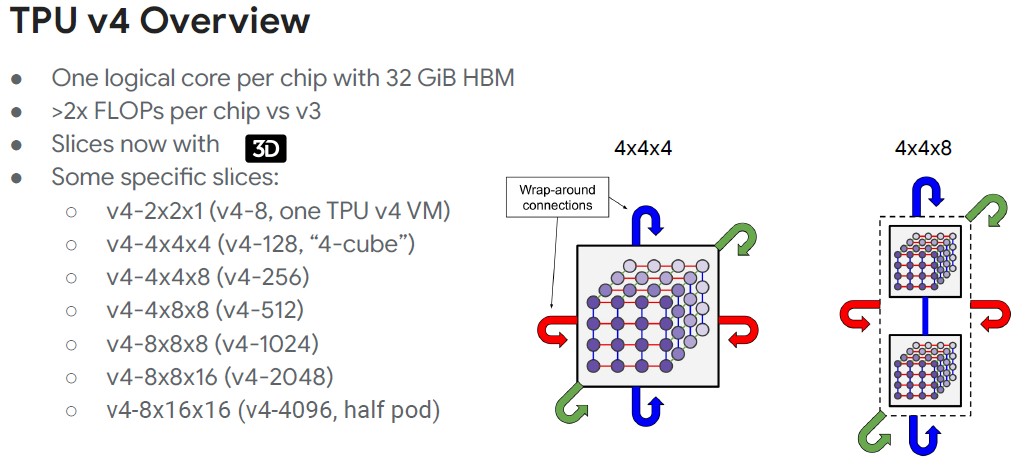
“In a lot of cases, engineers work with 64 chips or even a smaller number,” Vaibhav Singh, outbound product manager for the Cloud TPU offering at Google, tells The Next Platform. “One of the interesting things done with TPUv4 is this wraparound connection at the cube level, where the unit of a cube is four by four by four, because these are that was sort of our sweet spot in terms of the most frequent workload sizes. We can construct the larger slices as a composition of these four by four by four cubes.”
In the table above, the cube slice sizes are counting cores, not chips, so be careful in interpreting it. These slice sizes are dynamically configured.
“When we are talking about models that won’t fit into a single chip and have to be distributed across hundreds of chips, the awareness of that physical topology, and how tightly your software actually tries to do a certain set of optimizations in terms of the computation and communication overlaps makes a world of difference to the overall performance of the system,” Singh adds.
The HPC crowd is well aware of the benefits of 3D and higher dimension torus interconnects – IBM’s BlueGene supercomputers had a 3D torus and Fujitsu’s Tofu interconnect used in the K and Fukagu supercomputer were 6D torus/mesh interconnects – even if they are a pain in the neck to rewire if machines are added. (Hence the choice of a Clos or dragonfly topology for systems that need to be upgraded and rewired.)
Where The TPU Rubber Hits The AI Road
The TPUv4i and TPUv4, in particular against their predecessors and also against competing GPUs also aimed at AI training and inference, show the value of a minimalist design that only does one thing: Matrix math for AI processing. (Although we do know that there are some researchers that are trying to exploit TPUs to run accelerate HPC simulation and modeling applications.)
With the Hopper GPUs only now becoming generally available, the comparisons that Google was making using the TPUv4 engines versus other accelerators necessarily had to compare against Nvidia’s “Ampere” A100 GPUs. And the following charts, provided by Amin Vahdat, vice president of systems and services infrastructure at Google, show how a TPU stacks up against an A100 and how a TPUv4 pod on Google cloud stacks up against a similar sized cluster of A100s on Microsoft Azure.
These are research submission benchmarks of the MLPerf 2.0 suite of tests, which is the hot rod, nitro-guzzling version of the tests. Which is where the bleeding edge of AI is living. Here is the direct comparison between TPUv4 and A100 at different scales of compute engines (shown on the bars) for various neural network models:
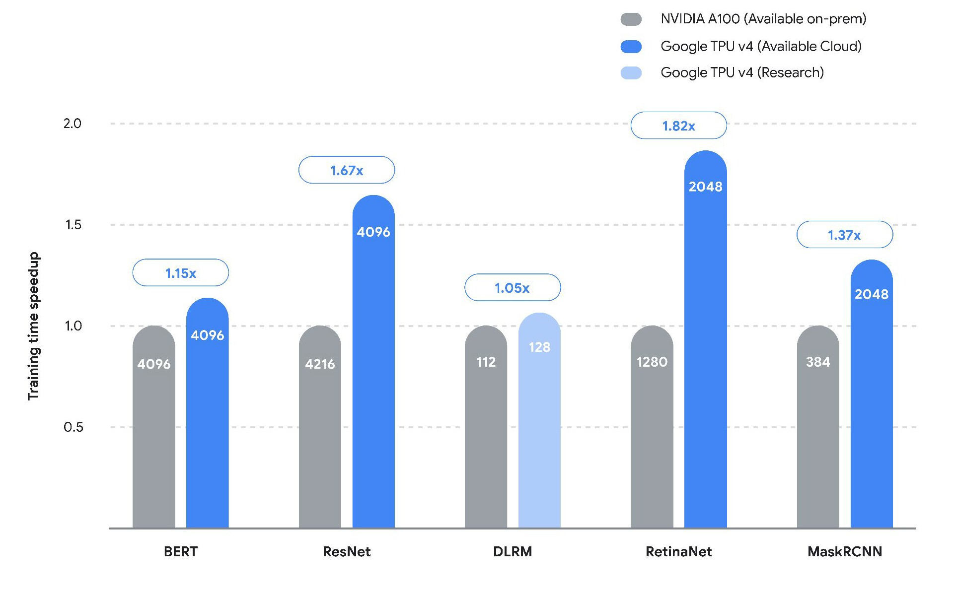
On lower scale models, the performance difference is not all that big as you see with Meta Platforms’ Deep Learning Recommendation Model (DLRM). A lot of times the performance gain seems to be due to the ability of the code to scale across more iron (as with the MaskRCNN and to a lesser extent RetinaNet) and sometimes it is due to scaling better on a large collection of iron (as with BERT and ResNet). On average, Vahdat says on the five benchmarks the TPUv4 had 40 percent higher performance on the MLPerf tests than the Nvidia A100s and, interestingly, the MLPerf 2.0 results that Google submitted on these five tests were 50 percent higher than on the same TPUv4 iron tested with the MLPerf 1.0 suite of tests.
“The point here is that actually these performance gains reflect software work, and a huge amount of optimization that we’re able to drive on our software, to take advantage of our hardware capabilities. That 50 percent relative to our last admission is particularly key because this means that all of our users for Cloud TPUs get those same performance benefits essentially for free.”
What matters, ultimately, and more than hardware feeds and speeds, is what AI training costs. And for once, Google gave us its own analysis of how its TPUv4 pod will stack up to a similarly sized cluster of machines using the same 4,096 Nvidia A100 GPUs:
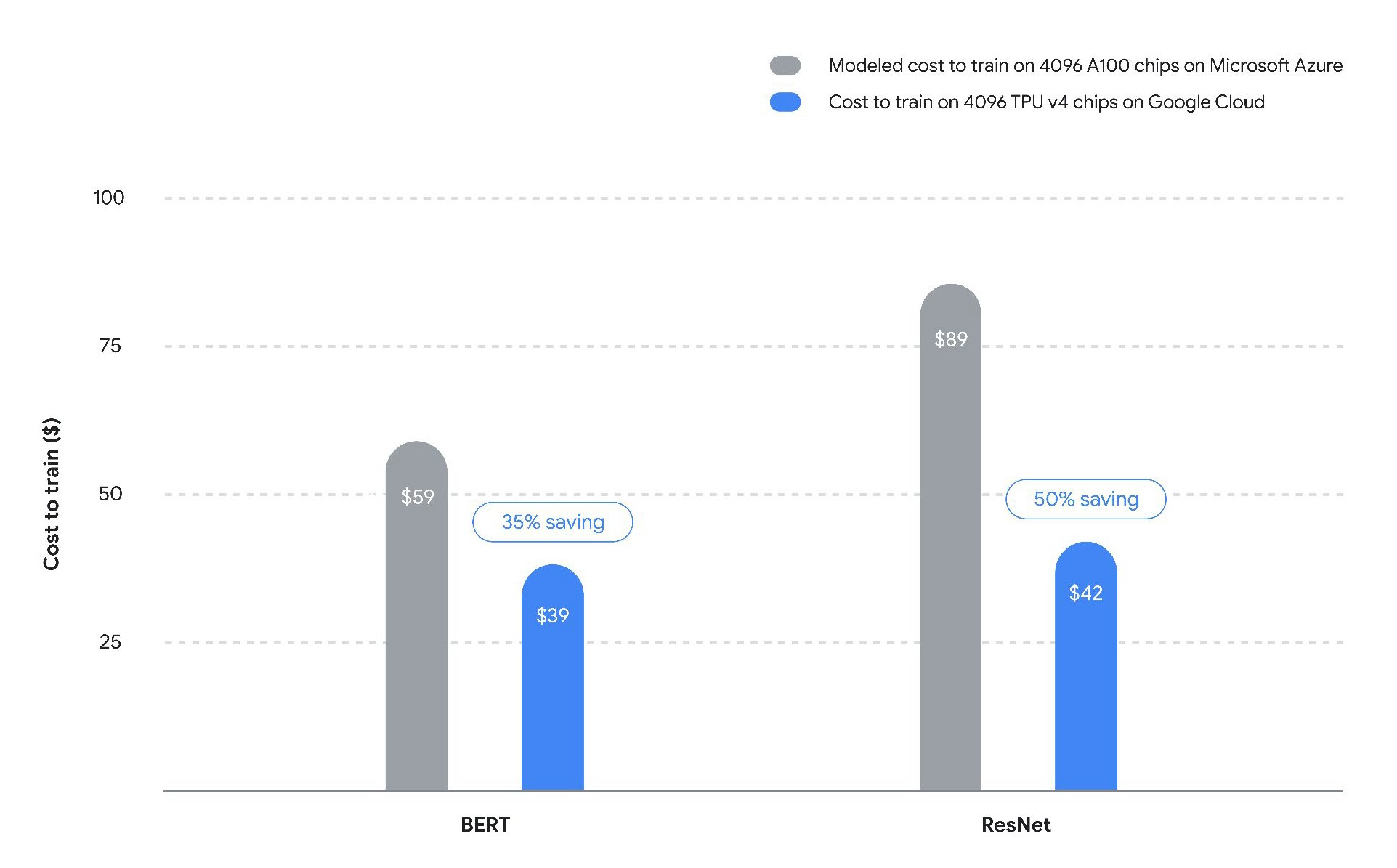
This cost was modeled by Vahdat’s team based on submitted MLPerf results and its own knowledge of how BERT and ResNet scale on GPUs – which Google sells and which Google still uses for plenty of its own AI workloads. It is unclear what a comparison to H100 GPU accelerators will look like. Nvidia might be offering 3X to 6X the performance (depending on the workload) for 2.5X to 3X the cost. (That is what it is looking like to us.) So Nvidia might close the scale and performance gap a bit, but not change the price/performance equation as much as you might think.
What we also find interesting is that the pricing for TPUv4 capacity is precisely what we expected it to be when we wrote back in May. The cost of an hour of time on a TPUv4 chip is 61 percent higher than for a TPUv3 chip, but it delivers 2.23X the performance. And so the price/performance improves by 28 percent. With the TPUv2 to TPUv3 jump, the performance went up 2.67 percent and the price/performance improved by 33.5 percent. This is consistent with the kind of bang for the buck improvements that Google likes to see and that customers expect generationally in the IT sector.


The Debate Over Regulating AI Ramps Up
Sundar Pichai, CEO of Google and parent company Alphabet, generated a lot of buzz recently with an op-ed he wrote for the The Financial Times calling for greater regulation of artificial intelligence (AI) technologies, adding a high-profile voice into a debate that has been simmering as innovation around AI, machine …
Quantum Computing Providers Pick Their Dance Partners
Toward the end of 2019, a flurry of announcements by some of the most prominent IT companies suggests that collaborations will become increasingly important in the quantum computing space as the players jockey for position in the nascent market. The companies in question include some of the biggest in the …

Vertical Integration Is Eating The Datacenter, Part Two
It is funny to think of the modern datacenter as an appliance, like an iPhone, but in the cases of the hyperscalers and the very largest public cloud builders, this is more or less what they are building. As we pointed out in the first part of this series, best …
The TPUv4 liquid cooling (parallel feeds) looks more apt than v3 (series) and v2 (air). Could it be a hint of higher TDP than previous models?
Not sure. Maybe the card is actually a lot smaller and there are 4X as many in a box?
Thank you for sharing this interesting article around TPU
For the tpu v4, does anyone know what the water flow rate is?
Or the physical size?
Hi, it seems that the recent TPUv4 paper that came out shows a surprising disparity between the numbers presented in the table.
https://arxiv.org/ftp/arxiv/papers/2304/2304.01433.pdf
I was pretty surprised to see that they were aiming for smaller die sizes (< 600mm2) and lower transistor count (22B) than all other competing designs in the 7nm category (typically 700-800mm2 with a 40-60B transistor count). I guess the targeting of a large "scale out" system (the 4K TPUv4s) made them put a greater emphasis on wires and interconnect than "scale up" compute ("beefier" systolic engines)?
Yeah, I am working on an analysis of that paper right now. Google could, I dunno, just answer questions when we ask them. It is supposed to be what the company does for a living (har har har).
The on chip SRAM size data of TPUv4 seems to wrong according there TPUv4 paper
“Like TPU v3, each TPU v4 contains two TensorCores (TC). Each TC contains four 128×128 Matrix Multiply Units (MXUs) and a Vector Processing Unit (VPU) with 128 lanes (16 ALUs per lane) and a 16 MiB Vector Memory (VMEM). The two TCs share a 128 MiB Common Memory
(CMEM).”
Total 160MB.