
What is the most important product that comes out of the semiconductor industry?
Here is a hint: It is inherent to the market, but enhanced by a positively reinforcing feedback loop of history. Here is another hint: You can’t hold it in your hand, like an A0 stepping of a device, and you can’t point at it like a foundry with the most advanced manufacturing processes created from $15 billion to $20 billion worth of concrete, steel, and wafer etching equipment and a whole lotta people in bunny suits.
No, the most important thing that the semiconductor industry delivers – and has consistently delivered for over five decades – is optimism. And unlike a lot of chips these days, there is no shortage of it despite the serious challenges that the industry is facing.
By optimism we do not mean the kind of “future poisoning” that company founders and chief executives sometimes succumb to when they spend too much time in the future that is not yet here without seeing the consequences of the technologies they are in the process of inventing. And we certainly do not mean the zeal that others exhibit when they think that information technology can solve all of our problems. It can’t, and it often makes some things worse as it is making other things better, as all technologies have done since humanity first picked up a stick. It is the arm that swings the stick both ways – to plant a seed or to crush a skull. So it is with the Internet, social media, artificial intelligence, and so on.
The optimism that we are speaking of in the semiconductor industry is usually stripped bare of such consequences, with the benefits all emphasized and the drawbacks mostly ignored – except possibly when considering the aspects of climate change and how compute, storage, and networking are an increasingly large part of our lives, and something that represents an ever-enlargening portion of business and personal budgets and consequently an embiggening part of the energy consumption on the planet. Semiconductor makers turn this drawback – more computers requiring more power and cooling – into a cause for driving innovation as hard as it can be done.
The irony is that we will need some of the most power-hungry systems the world has ever seen to simulate the conditions that will prove how climate change will affect us collectively and – here is the important bit – individually. How will you feel when you can drill down into a simulation, for a modest fee of course, and see a digital twin of your home being destroyed by a predicted hurricane two years from now? Or an earthquake, or a fire, or a tsunami? What is true of the Earth simulation will be as true for your body simulation and your consequent healthcare.
If the metaverse means anything, it means using HPC and AI to make general concepts extremely personal. We don’t know that the world was hell bent to adopt the 24 hour news cycle and extreme entertainment optionality of cable television, or the Web, or social networks, but what we do know is that most of us ended up on these platforms anyway. And what seems clear is that immersive, simulated experiences are going to be normalized, are going to be a tool in all aspects of our lives, and that the race is on to develop the technologies that will get us there.
Catalyzing The Impossible
It would be hard to find someone more genuine and more optimistic about the future of the semiconductor industry than Aart de Geus, co-founder, chief executive officer, and chairman of electronic design automation tool maker Synopsys, who gave the opening keynote at the ISSCC 2022 chip conference, which was hosted online this week. We read the paper that de Geus presented and watched the keynote as well, and will do our best to summarize the tour de force in semiconductor history and prognostication as we enter in what de Geus called the SysMoore Era – the confluence of Moore’s Law ambitions in transistor design and now packaging coupled to systemic complexity that together will bring about a 1,000X increase in compute across devices and systems of all kinds and lead to a “smart everything” world.
Here is de Geus showing the well familiar exponential plot of the transistor density of CPUs, starting with the Intel 4004 in 1971 and running all the way out five decades later to the Intel “Ponte Vecchio” GPU complex, with 47 chiplets lashing together 100 billion transistors, and the Cerebras WSE 2 wafer-scale processor, with 2.5 trillion transistors.
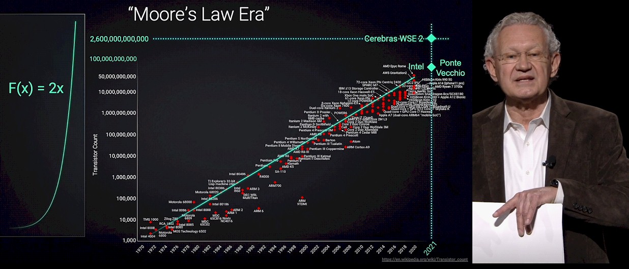
That’s the very familiar part of the SysMoore Era, of course. The Sys part needs a little explaining, but it is something that we have all been wrestling with in our next platforms. Moore’s Law improvements of 2X transistor density are taking bigger leaps to stay on track and are not yielding a 2X lowering in the cost of the transistors. This latter bit is what actually drives the semiconductor industry (aside from optimism), and we are now entering a time when the cost of transistors could rise a little with each generation, which is why we are resorting to chiplets and advanced packaging to glue them together side-by-side with 2.5D interposers or stacking them up in 3D fashion with vias – or in many cases, a mix of the two approaches. Chiplets are smaller and have higher yield, but there is complexity and cost in the 2.5D and 3D packaging. The consensus, excepting Cerebras, is that this chiplet approach will yield the best “tech-onomic” results, to use a term from de Geus.
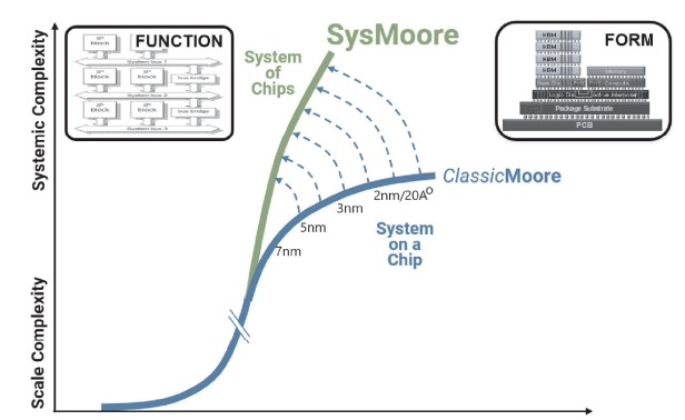
With SysMoore, we are moving from system on chip designs to system of chips designs, illustrated below, to bend up the semiconductor innovation curve that has been dominated by Moore’s Law for so long (with some help from Dennard scaling until 2000 or so, of course). Like this:
The one thing that is not on the charts that de Geus showed in the keynote, and that we want to inject as an idea, is that compute engines and other kinds of ASICs are definitely going to get more expensive even if the cost of packing up chiplets or building wafer-scale systems does not consume all of the benefits from higher yield that comes from using gangs of smaller chips or adding lots of redundancy into a circuit and never cutting it up.
By necessity, as the industry co-designs hardware and software together to wring the most performance per dollar per watt out of a system, we will move away from the volume economics of mass manufacturing. Up until now, a compute engine or network ASIC might have hundreds of thousands to millions of units, driving up yields over time and driving down manufacturing cost per unit. But in this SysMoore Era, volumes for any given semiconductor complex will go down because they are not general purpose, like the X86 processor in servers and PCs or the Arm system on chip was for smartphones and tablet have both been for the past decade and a half. If volumes per type of device go down by an order of magnitude, and the industry needs to make more types devices, this will put upward pressure on unit costs, too.
So what is the answer to these perplexing dilemmas that the semiconductor industry is facing? Artificial intelligence augmenting human expertise in designing these future “system of chips” complexes, of course. And it is interesting that the pattern that evolved to create machine learning for data analytics is being repeated in chip design.
“EDA is relatively simple conceptually,” explains de Geus. “If you can capture data, you may be able to model it. If you can model it, maybe you can simulate. If you can simulate, maybe you can analyze. If you can analyze, maybe you can optimize. And if you can optimize, maybe you can automate. Actually, let’s not forget the best automation is IP reuse – it is the fastest, most efficient kind. Now it’s interesting to observe this because if you look at the bottom layers, what we have been doing in our field really for 50 years, is we have built digital twins of the thing that we are still building. And if we now say we’re going to deliver to our customers and the world that 1,000X more capability in chips, the notion of Metaverse – some call it Omniverse, Neoverse, whatever you want to call it – is becoming extremely powerful because it is a digital view of the world as a simulation of it.”
The complexity that comprises a modern chip complex, full of chiplets and packaging, is mind-numbing and the pressure to create the most efficient implementation, across its many possible variations, is what is driving the next level of AI-assisted automation. We are moving from computer-aided design, where a workstation helped a chip designer, to electronic design automation, where synthesis of logic and the placing and routing of that logic and its memories and interconnects, is done by tools such as those supplied by Synopsys, to what we would call AIDA, short for Artificial Intelligence Design Automation, and making us think of Ada Lovelace, of course, the programmer on the Difference Engine from Charles Babbage.
This chart captures the scale of complexity in an interesting way, since the bottom two have been automated by computers – IBM’s Deep Blue using brute force algorithms to play chess and Google’s AlphaGo using AI reinforcement learning to play Go.

Google has been using lessons learned from AlphaGo to do placement and routing of logic blocks on chips, as we reported two years ago from ISSCC 2020, and Synposys is embedding AI in all parts of its tool stack in something it is calling Design Space Optimization, or DSO. A chess match has a large number of possible moves, and Go has orders of magnitude more, but both are “win-loss” algorithms. Not so for route and placement of logic blocks or the possible ways to glue compute complexes together from myriad parts. These are not zero sum algorithms, but merely better or worse options, like going to the eye doctor and sitting behind that annoying machine with all the blasted lenses.
The possible combinations of logic elements and interconnects is a very large data space, and will itself require an immense amount of computation to add AI to the design stack. The amount has been increasing on a log scale since the first CAD tools became widely used:
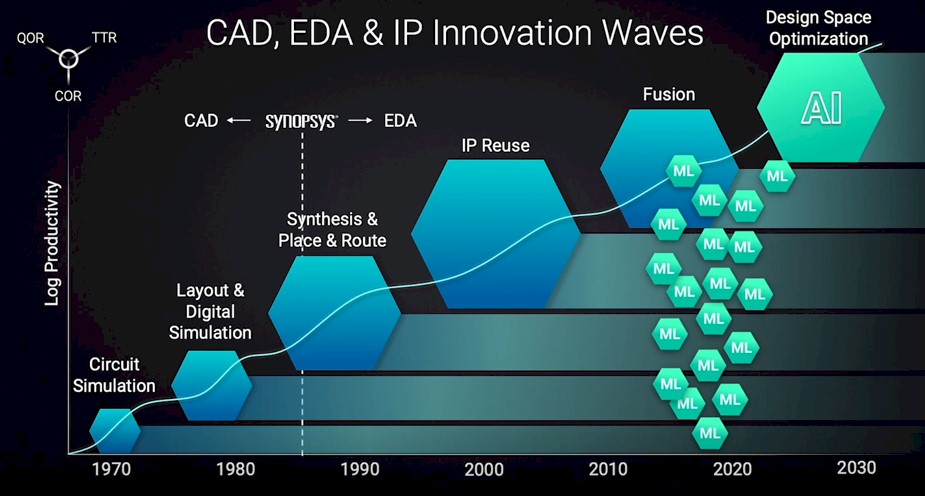
But the good news is that the productivity gains from chip design tools have been growing at a log scale, too. Which means what you can do with one person and one workstation designing a chip is amazing here in the 2020s. And will very likely be downright amazing in the 2030s, if the vision of de Geus and his competitors comes to pass.
In the chart above, the Fusion block is significant, says de Geus, and it is implemented in something called the Fusion Compiler in the Synopsys toolchain, and this is the foundation for the next step, which is DSO. Fusion plugs all of these different tools together to share data as designers optimize a chip for power, performance, and area – or PPA, in the lingo. These different tools work together, but they also fight, and they can be made to provide more optimal results than using the tools in a serial manner, as this shows:
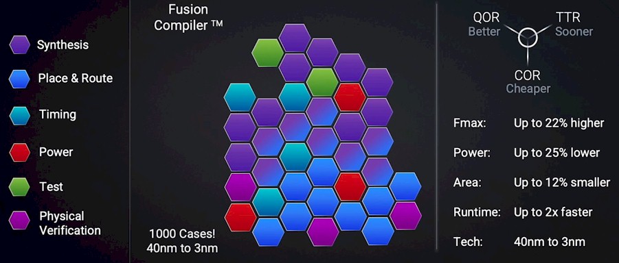
The data shown above is an average of more than 1,000 chip designs, spanning from 40 nanometers down to 3 nanometers. With DSO, machine learning is embedded in all of the individual elements of the Fusion Compiler, and output from simulations is used to drive machine learning training that in turn is used to drive designs. The way we conceive of this – and de Geus did not say this – is that the more the Synopsys tools design chips and examine options in the design space, the faster it will learn what works and what does not and the better it will be at showing human chip designers how to push their designs.
Let’s show some examples of how the early stages of DSO works with the Synopsys tools, beginning with a real microcontroller from a real customer:
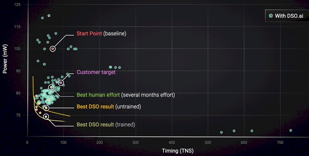
De Geus highlighted the important parts of the design, with a baseline of the prior design and the target of the new design. A team of people were set loose on the problem using the Synopsys tools, and you can see that they beat the customer target on both power and timing by a little bit. Call it a day. But then Synopsys fired up the Fusion Compiler and its DSO AI extensions. Just using the DSO extensions to Fusion pushed the power draw down a lot and to the left a little, and then once AI trained algorithms were kicked on, the power was pushed down even further. You can see the “banana curve” for the DSO and DSO AI simulations, which allows designers to trade off power and timing on the chip along those curves.
Here is another design run that was done for an actual CPU as it was being designed a year ago:
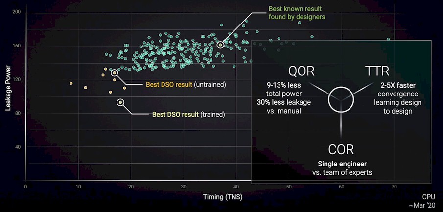
A team of experts took months to balance out the power leakage versus the timing in the CPU design. The DSO extensions to the Fusion Compiler pushed it way over to the left and down a little, and when the AI trained models of the tool were switched on, a new set of power leakage and timing options were shown to be possible. A single engineer did the DSO design compared to a team using the Synopsys tools, and that single engineer was able to get a design that burned from 9 percent to 13 percent less power and had 30 percent less power leakage – with anywhere from 2X to 5X faster time to design completion.
There were many more examples in the keynote of such advances after an injection of AI into the tools. But here is the thing, and de Geus emphasized this a number of times. The cumulative nature of these advances are not additive, but multiplicative. They will amplify much more than the percents of improvement on many different design vectors might imply. But it is more than that, according to de Geus.
“The hand that develops the computer on which EDA is written can help develop the next computer to write better EDA, and so on,” de Geus explained at the end of his talk. “That circle has brought about exponential achievements. So often we say that success is the sum of our efforts. No, it’s not. It is the product of our efforts. A single zero, and we all sink. Great collaboration, and we all soar.”

Getting To Zettascale Without Needing Multiple Nuclear Power Plants
There’s no resting on your laurels in the HPC world, no time to sit back and bask in a hard-won accomplishment that was years in the making. The ticker tape has only now been swept up in the wake of the long-awaited celebration last year of finally reaching the exascale …
What Do We Do When Compute And Memory Stop Getting Cheaper?
The IT industry, like every other industry we suppose, is in a constant state of dealing with the next bottleneck. It is a perpetual game of Whac-a-Mole – a pessimist might say Sisyphusian at its core, an optimist probably tries not to think about it too hard and deal with …
Synopsys Shepherds Circuits Towards 1.6T Ethernet
The Ethernet roadmap has had a few bumps and potholes in the four and a half decades since the 10M generation was first published in 1980. Remember the long time between 10 Gb/sec to 100 Gb/sec and the 40 Gb/sec bridge between the two that represented the first time we …
Be the first to comment