

We made a joke – sort of – many years ago when we started this publication that the future compute engines would look more like a GPU card than they did a server as we knew it back then. And one of the central tenets of that belief is that, given how many HPC and AI applications are bound by memory bandwidth – not compute capacity or even memory capacity – that some form of extremely close, very high bandwidth memory would come to all manner of calculating chips: GPUs, CPUs, FPGAs, vector engines, whatever.
This has turned out to be largely true, at least for now until another memory approach is invented. And if the FPGA – more accurately, hybrid compute and networking complexes that we call FPGAs even though they are much more than programmable logic blocks – is going to compete for compute jobs, it is going to have to have some form of high bandwidth main memory tightly coupled to it. Which is why Xilinx is now talking about its high-end Versal HBM device, which has been hinted at in the Xilinx roadmaps since 2018 and which is coming to market in about nine months, Mike Thompson, senior product line manager for the beefy Virtex UltraScale+ and Versal Premium and HBM ACAPs at Xilinx, tells The Next Platform. That is about six months later than expected – it is hard to say with the vagaries of the X axis on many vendor roadmaps as they get further way from the Y axis, but estimate for yourself: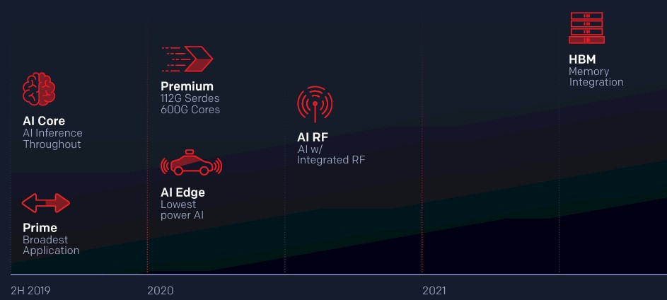
Xilinx has been blazing the high bandwidth main memory trail along with a few other device makers, and not as a science experiment but because many latency sensitive workloads in the networking, aerospace and defense, telecom, and financial services industries simply cannot get the job done with standard DRAM or even the very fast SRAMs that are embedded in FPGA logic blocks.
High bandwidth memory originally came in two flavors for datacenter compute engines, but the market has rallied around one of them.
The MCDRAM variant called Hybrid Memory Cube (HMC) from Intel and Micron Technology was deployed on the Intel “Knights Landing” Xeon Phi devices, which could be used as compute engines in their own right or as accelerators for plain vanilla CPUs. The Xeon Phi could deliver a little more than 400 GB/sec of memory bandwidth across 16 GB of HMC memory to the heavily vectorized Atom cores on the chip, which was significant for the time. This HMC variant was also used in the Sparc64-IXfx processor from Fujitsu, which was aimed at supercomputers, which had 32 GB of capacity, and which delivered 480 GB/sec of bandwidth across its four memory banks.
But with the A64FX Arm-based processor that Fujitsu, designed for the “Fugaku” supercomputer that is the world’s most powerful machine, Fujitsu switched to the more common second-generation High Bandwidth Memory (HBM2) variant of stacked, parallel DRAM, which was initially created by AMD and memory makers Samsung and SK Hynix and first used in the “Fiji” generation of Radeon graphics cards about the same time Intel was rolling out the Xeon Phi chips with MCDRAM in 2015.
Fujitsu put four channels on the chip that delivered 32 GB of capacity and a very respectable 1 TB/sec of bandwidth – an order of magnitude or so more than a CPU socket delivers, just to put that into perspective.
Given the need for high bandwidth and larger capacity than integrated SRAM could offer, Xilinx put 16 GB of HBM2 memory, delivering 460 GB/sec of bandwidth, on its prior generation of Virtex UltraScale+ FPGAs. As you can see, this is about half of what the flops-heavy CPU compute engines of the time were offering, and you will see this pattern again. The speed is balanced against the needs of the workloads and the price point that customers need. Those buying beefy FPGAs have just as much need for high speed SerDes for signaling, so they have to trade off networking and memory to stay within a thermal envelope that makes sense for the use cases.
Nvidia has taken HBM capacity and bandwidth to extremes as it has delivered three generations of HBM2 memory on its GPU accelerators, with the current “Ampere” devices having a maximum of 80 GB of capacity yielding a very impressive 2 TB/sec of bandwidth. And this need for speed – and capacity – is being driven by flops-ravenous AI workloads, which have exploding datasets to chew on. HPC codes running on hybrid CPU-GPU systems can live in smaller memory footprints than many AI codes, which is fortunate, but that will not remain true if the memory is available. All applications and datasets eventually expand to consume all capacities and bandwidths.
Some devices fit in the middle of these two extremes when it comes to HBM memory. NEC’s “Aurora” vector accelerators launched four years ago had 48 GB of HBM2 memory and 1.2 TB/sec of bandwidth, beating the “Volta” generation of GPU accelerators from Nvidia of the time. But the updated Ampere’s launched this year just blow everything else away in terms of HBM2 capacity and bandwidth. Intel has just announced that its future “Sapphire Rapids” Xeon SP processors, now expected next year, will have a variant that supports HBM2 memory, and of course the companion Ponte Vecchio” Xe HPC GPU accelerator from Intel will have HBM2 memory stacks, too. We don’t know where Intel will end up on the HBM2 spectrum with its CPUs and GPUs, but probably somewhere between the extremes for the CPUs and near the extremes for the GPUs if Intel is truly serious about competing.
The forthcoming Versal HBM devices from Xilinx are taking a middle way course as well, for the same reasons that the Virtex UltraScale+ devices did when they were unveiled in November 2016. But Xilinx is also adding in other HBM innovations that reduce latency further than other do per unit of capacity and bandwidth.
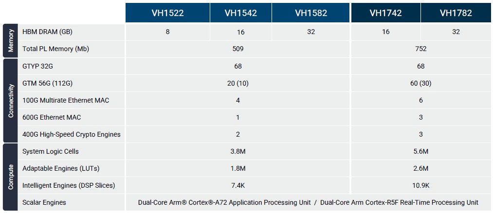
The Versal HBM device is based on the Versal Premium device, which we detailed in March 2020. That Versal Premium complex has four super logic regions, or SLRs as Xilinx calls them, and one of these SLRs is swapped out with two banks of eight-stacks of HBM2e memory. Each stack has a maximum of 16 GB for a total of 32 GB, and memory across the SKUs is available in 8 GB, 16 GB, and 32 GB with varying amounts of compute and interconnect. The SLR immediately adjacent to the swapped in HBM memory has an HBM controller and an HBM switch – both of which are designed by Xilinx –embedded in it, which Thompson says is relatively small. This HBM switch is a key differentiator.
“One of the challenges with HBM is that you can’t access every memory location from any of the memory ports, and we have 32 memory ports on this device,” explains Thompson. “Other products in the market do not build in a switch, either, which means they have to spend a large amount of soft logic to create a switch of their own, which eats a significant chunk of the logic in these devices and somewhere between 4 watts and 5 watts of power. With other devices using HBM, not having a switch causes massive overhead and additional latency as memory maps end up being much more annoying than they should be.”
Yet another piece of the FPGA logic being hard-coded in transistors for efficiency, along with the SerDes and many other accelerators. Here is what the Versal HBM block diagram looks like:
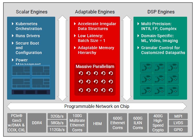
As with the Versal Premium devices, the Versal HBM devices have some scalar processing engines based on Arm cores, some programmable logic that implements the FPGA functionality and its internal and various memories, and DSP engines that do mixed-precision math for machine learning, imaging, and signal processing applications. Attached to this is the HBM memory and a slew of hard-coded I/O controllers and SerDes that make data zip into and out of these chips at lightning speed. One of the reasons why FPGA customers need HBM memory on such a device is because it has so much different I/O adding up to so much aggregate bandwidth. The PCI-Express 5.0 controllers, which support DMA, CCIX, and CXL protocols for memory latency, have an aggregate of 1.5 Tb/sec of bandwidth; and the chip-to-chip Interlaken interconnect has an integrated forward error correction (FEC) accelerator and deliver 600 Gb/sec of aggregate bandwidth. The cryptographic engines, which are also hard-coded like the PCI-Express and Interlaken controllers, support AES-GCM at 128 bits and 256 bits as well as MACsec and IPsec protocols, and deliver 1.2 Tb/sec of aggregate bandwidth and can do encryption at 400 Gb/sec to match the line rate of a 400 Gb/sec Ethernet port. The hard-coded Ethernet controllers can drive 400 Gb/sec ports (with 58Gb/sec PAM4 signaling) and 800 Gb/sec ports (with 112 Gb/sec PAM4 signaling) as well as anything down to 10 Gb/sec along the Ethernet steps using legacy 32 Gb/sec NRZ signaling; all told, the chip has an aggregate Ethernet bandwidth of 2.4 Tb/sec.
This Versal HBM device is a bandwidth beast on I/O, and for certain applications, that means it needs to be a memory bandwidth beast to balance it out. And the Versal HBM device is much more of a beast than the Virtex UltraScale+ HBM device it will replace, and proves it on many different metrics beyond HBM memory capacity and bandwidth. This is enabled through architectural changes and the shift from 16 nanometer processes down to 7 nanometers (thanks to fab partner Taiwan Semiconductor Manufacturing Corp).
Thompson says the Versal HBM device has the equivalent of 14 FPGAs of logic and the HBM has the equivalent bandwidth as 32 DDR5-6400 DRAM modules.
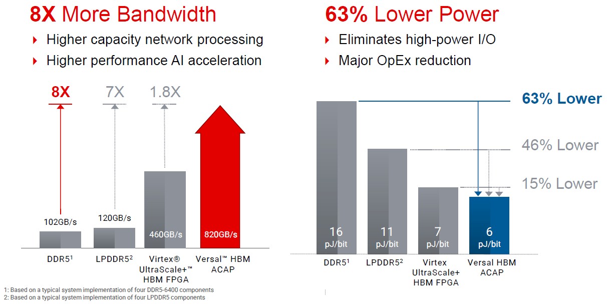
The device has 8X the memory bandwidth and uses 63 percent less power than four DDR5-6400 modules of the same capacity, Xilinx estimates:
So how will the Versal HBM device stack up against prior Xilinx devices and Intel Agilex devices and Intel and AMD CPUs? Well, you can forget any comparisons to AMD Epyc CPUs with AMD in the middle of buying Xilinx for $35 billion. And Thompson did not bring any comparisons to Intel ACAP-equivalent devices, either. But he did bring some charts that pit two-socket Intel “Ice Lake” Xeon SP systems against the Virtex HBM and Versal HBM devices, and here is what it looks like:
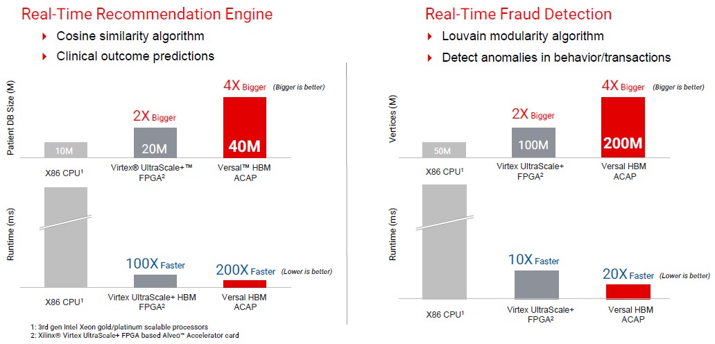
On the clinical records recommendation engine test on the left of the chart above, the CPU-only system takes seconds to minutes to run, but the old Virtex HBM device was able to hold a database that was twice as large because of the speed at which it could stream data into the device and was 100X faster at making recommendations for treatments. The Versal HBM device held a database twice as large and derived the recommendations twice as fast. The same relative performance was seen with the real-time fraud detection benchmark on the right.
Here is another way to think about how the Versal HBM device might be used, says Thompson. Say you want to build a next-generation 800 Gb/sec firewall that has machine learning smarts built in. If you want to employ the Marvell Octeon network processor SoC, which can only drive 400 Gb/sec ports, you will need two of them, and they do not have machine learning. So you will need two Virtex UltraScale+ FPGAs to add that functionality to the pair of Octeons. It will also take a dozen DDR4 DRAM modules to deliver 250 GB/sec of memory throughput. Like this:
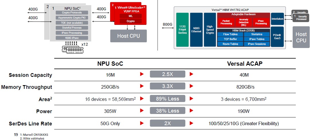
Presumably, not only is the Versal HBM system better in terms of having fewer devices, more throughput, and less power consumption, but is also less expensive to buy, too. We don’t know because Xilinx does not give out pricing. And if not, it surely has to deliver better bang for the buck and better performance per dollar per watt or there is no sense in playing this game at all. By how much, we would love to know.


The Fourth Wave Of FPGA Compute
Ahead of The Next FPGA Platform event that we hosted recently in San Jose, we talked to Manoj Roge, vice president of product planning and business development at Achronix, about the three waves of FPGAs that have occurred over the past three decades, and in the course of our live …
What Gelsinger Can Do To Unscrew Intel
A little more than a week ago, Intel announced that Pat Gelsinger, its former chief technology officer and former manager of the predecessor of its Data Center Group as well as the current chief executive officer at server virtualization juggernaut VMware, would be returning to the world’s biggest chip maker …

The Killer Apps For FPGAs Could Be SmartNICs And Storage
If FPGAs are going to take off in the datacenter in their own right, they are going to need their own killer apps. Plural. At The Next FPGA Platform event that we hosted recently in San Jose, there was plenty of talk about how FPGAs have been embedded in all …
“And Thompson did not bring any comparisons to Intel ACAP-equivalent devices, either”… I wonder why Xilinx is scared of comparing their products to Intel’s Agilex.
Very Nice Article. Can you please provide details of application which require High Memory Bandwidth.