
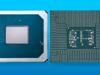
It has been a long time since plain vanilla programmable logic circuits known as field programmable gate arrays have been available in a raw form. For many years, Xilinx, Altera, and others making what we call FPGAs have been adding hard-coded circuits for certain functions that might otherwise be synthesized from gates, and perhaps more than any other discrete device sold today, what we call an FPGA is a true system on chip, with all kinds of compute, memory, and interconnect resources all expressed in the transistors of the device.
Companies are not creating these hybrid compute devices because they like complexity, but rather because customers who are looking for an edge in compute want to exploit the malleable compute capability inherent in the FPGA while getting some of the ease of programming and speed of ASIC blocks. It is a tough balance across a single device, much less a line of devices aimed at different sectors of the IT space. This is why Xilinx calls its most recent devices, the “Everest” line of chips that began rolling out in October 2018, Adaptive Compute Acceleration Platforms, or ACAPs. We doubt very much that the name will catch on and that people will still call them FPGAs. The important thing is that Xilinx has rolled out the next – and more powerful – FPGA in the Everest Versal series, following up on the FPGA-based SmartNIC in the Alveo line that was announced last week.
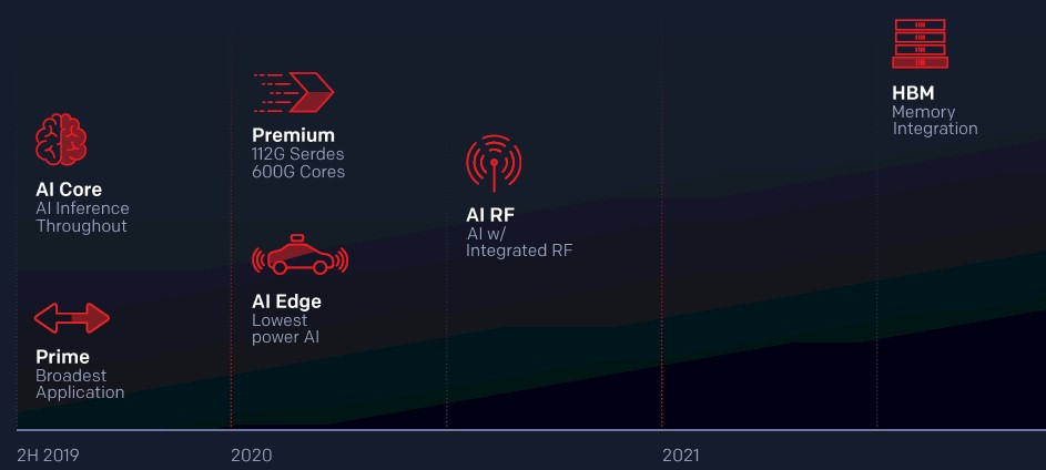
In the Versal AI Core and Versal Prime devices were the first out the door, shipping in the middle of last year, and the new Versal Premium device is a beefed up version of the Versal Prime that is intended for heftier datacenter workloads and are the follow-on to the Virtex UltraScale+ FPGAs that Xilinx has been selling for a number of years now. Speaking very generally, the Versal Premium devices are designed to be used in public and private cloud acceleration for a wide variety of workloads that need more oomph on various compute, storage, and networking elements than is possible with the Versal Prime or Virtex UltraScale+ devices. The Versal Premiums are also aimed at core and regional networking and access and metro networking applications in the telco and service provider sectors. These beefy Versal units do not, however, support HBM memory. The Versal HBM Series is still to come, slated for delivery at the end of 2021 or so according to the Xilinx roadmap.
To refresh, here is the Versal roadmap:
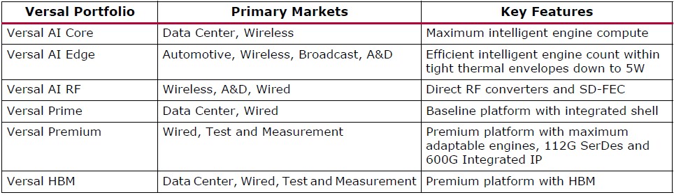
And here is the table describing the different characteristics of the families of Versal devices:
That core network is going to be a big consumer of the Versal Premium devices, according to Mike Thompson, senior product line manager of high-end FPGAs and ACAPs at Xilinx. Thompson cites data from the 2019 Global Interconnection Index report from datacenter operator Equinix that shows the bandwidth requirements on the core network are growing at a compound annual growth rate of 51 percent between 2018 and 2022, inclusive, reaching 13,300 Tb/sec globally. Enterprises will make up a little more than half of that core network capacity, and service providers the rest.
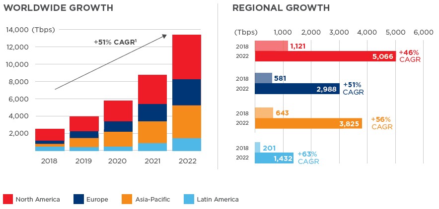
“There is an explosion of data from all kinds of workloads that are putting tremendous pressure on the core network, which now I would say includes the core datacenters as well as the core transport and metro networks,” Thompson tells The Next Platform. “This bandwidth demand is coming from video streaming, from enterprise applications that are increasingly hyperscale datacenter centric, smart devices having broadband connections as well as IoT devices. Nominally, year over year, that is up by 50 percent and every two years it more than doubles. I have been in this industry for a long time, and keeping pace with that is hard enough, but with 5G devices we are going to see 100X increase in bandwidth demand at the access layer of the network because there will be an order of magnitude increase in the number of devices and another order of magnitude increase in the bandwidth to each device. I would argue that this is a conservative estimate, and it could be as high as 1,000X more bandwidth needed at the access layer.”
This need to handle so much more data at the core and access layers is one of the drivers in the communications sector business at Xilinx, Thompson adds.
Before getting into the specifics of the Versal Premium devices, which will start sampling in the first half of 2021 and which have customers that need a very long lead time to absorb new technologies, it is probably a good idea to review the Versal architecture and then talk about how the Premium devices are different from the currently shipping Prime and AI Core devices.
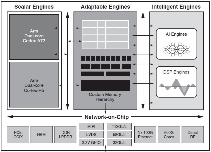
The Versal devices are indeed versatile, and they have many different kinds of compute, memory, and networking all embedded on a single device. On the compute front, there are four different kinds of engines. For scalar processing, there is a dual-core Arm Cortex-A72 chip for relatively heavy workloads and a dual-core Cortex-A5F for lighter workloads. The so-called intelligent engines are hard blocks of transistors that are woven together as DSPs or as what Xilinx calls AI Engines, which are really matrix math units aimed at machine learning workloads (mostly lower precision inference). In the adaptable engines, which is the core FPGA functionality, there are the Look Up Tables (LUTs) that implement the malleable gate logic but which also can be configured as LUT RAM memory that is embedded in the logic. This is a very useful feature of FPGAs and is sometimes called distributed RAM. The adaptable logic also has embedded block RAM scattered around the gates, and giant fatter columns of memory called UltraRAM that debuted with the prior generations of UltraScale+ devices from 2016. All told, the block RAM and UltraRAM capacity on the Versal Premium device delivers 123 GB/sec of aggregate memory bandwidth inside of the FPGA fabric. By comparison, the caches inside of the Nvidia Tesla V100 GPU accelerator have an aggregate of 14 TB/sec of on-chip memory bandwidth and the caches in the smaller Tesla T4 accelerator weight in at only 5 TB/sec. (This is not the bandwidth into and out of the chips, which the Tesla V100 GPU would surely win, at least until Xilinx gets an HBM version of its Versal series out the door.)
Now, for workloads that need more than a few hundred megabits of memory capacity within the FPGA fabric, the Versal architecture has hard coded DDR4 memory controllers, and this is a bit distinct from the soft-coded external memory controllers that often burned a lot of LUTs to be implemented on prior generations of devices from Xilinx. For instance, on the Virtex UltraScale+ VU9P device, about a third of the LUTs – about 200,000 of them – on the device were used to implement four memory controllers and a PCI-Express plus DMA controller. With the Versal Premium generation, these controllers are hard coded and burn no LUTs at all. Eventually, Xilinx will ship devices with HBM stack memory, but that is not for a while yet.
The PCI-Express 5.0 controller support DMA operations as well as the CCIX accelerator memory coherency protocol that Xilinx has been spearheading for four years and that the Arm collective is starting to adopt as the NUMA interconnect between processors running over the PCI-Express bus. The PCI-Express 5.0 controllers will also sport Intel’s CXL protocol for coherent accelerator attachment.

The Versal devices are also equipped with had block SerDes circuits that support PAM4 signaling running at 112 Gb/sec, which can be used to support raw Ethernet and Interlaken (a streamlined chip-to-chip, packet-based interconnect used in communications gear created by Cisco Systems and Cortina Systems back in 2006). Both Xilinx and Intel/Altera devices support high speed Interlaken ports on their respective FPGAs, which allows them to be linked together in a fashion that is analogous to (but distinct from) NUMA interconnect in CPUs. The Versal Premium devices have 600 Gb/sec Ethernet ports based on these 112 Gb/sec SerDes as well as 600 Gb/sec Interlaken. The chips also sport 32 Gb/sec SerDes that employ non-zero return (NRZ) signaling and 58 Gb/sec SerDes that support 58 Gb/sec PAM4 signaling. The 32 Gb/sec ports are used for Ethernet ports running at between 10 Gb/sec and 100 Gb/sec, while the 58 Gb/sec ports are used to create 400 Gb/sec ports. The 112 Gb/sec ports are aimed at future 800 Gb/sec Ethernet as well as the Interlaken links.
Given that these devices are not expected to do a lot of heavy lifting with machine learning – Xilinx will have other Versal packages to do this – they do not have hard-coded AI engines, but they do have hard coded DSP engines. Additionally, the Premium devices have cryptographic engines that can encrypt and decrypt data at 400 Gb/sec line rate speeds.
The Versal Premium devices are absolutely aimed at the telecom and communications sector, and the idea is to embed the FPGAs into networking devices that span from the access layer to the core and all with the same underlying hardware capability – importantly with line rate security and the FPGA functions for machine learning and anomaly detection – and a consistent Vitis programming environment for the FPGAs across all layers of the network. Like this:
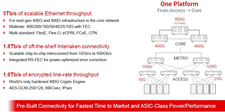
There are a bunch of different forces that are putting the squeeze on telcos and service providers. That 5G edge is going to put pressure on the core network, and the floor space in points of presence is not going to increase. So the density of networking bandwidth and the compute that is increasingly associated with it is going to have to go up, and so is the electrical and thermal efficiency. Here is just one example of a network line card use case for a Versal Premium FPGA:
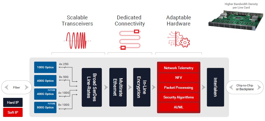
Now, you can see how all the different elements of the Versal Premium device comes into play. We can drill down further into the red part of the diagram and talk about how the programmable logic can be used to run AI inference for specific network workloads:
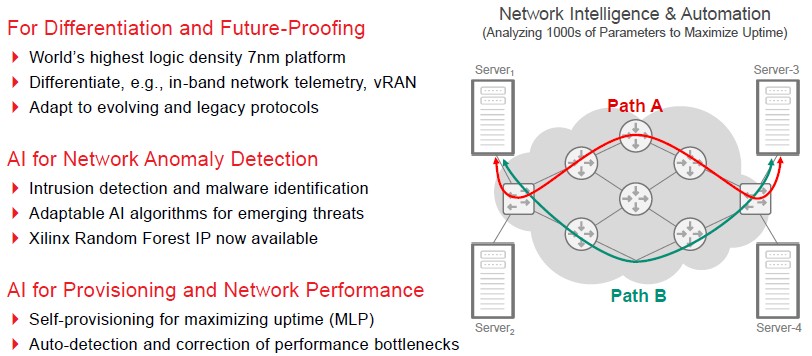
There are so many changing patterns in the network that machine learning almost has to be a part of the network devices just so the complexity can be dealt with in real-time to keep the network humming along. On image classification inference workloads running the ResNet neural network, the top-end Versal Premium VP1802 can do about 60 percent more image classification throughput than an Nvidia Tesla V100 and about 130 percent more than an Nvidia Tesla T4. The gap with the Yolov2 object detection neural network is more like 4.6X and 7.7X respectively. That gives a sense of the raw inference performance here and what might happen if image recognition workloads were dumped onto the network. But as far as network jobs go, the anomaly detection workload that Xilinx ran on the Versal Premium VP1802, which measured the predictions per second using a random forest method, a single VP1802 device was 280X faster than a 16-core Xeon E5-2687W processor running at 3.4 GHz. That is about 310X the performance of the current “Cascade Lake-R” Xeon SP-6259 Gold processor, which has eight cores running at 3.9 GHz, if you want to translate it to the current Intel chips. That chip costs $3,400. You could spread it across more cores in a cheaper processor and close the gap between X86 and FPGA, but the gap would still be huge, on the order of 200X at about half that price. Clock speed really costs a lot with Intel processors, and indeed with any processors.
The Versal Premium line of FPGAs (again, using that term loosely) has seven different variants, as follows:
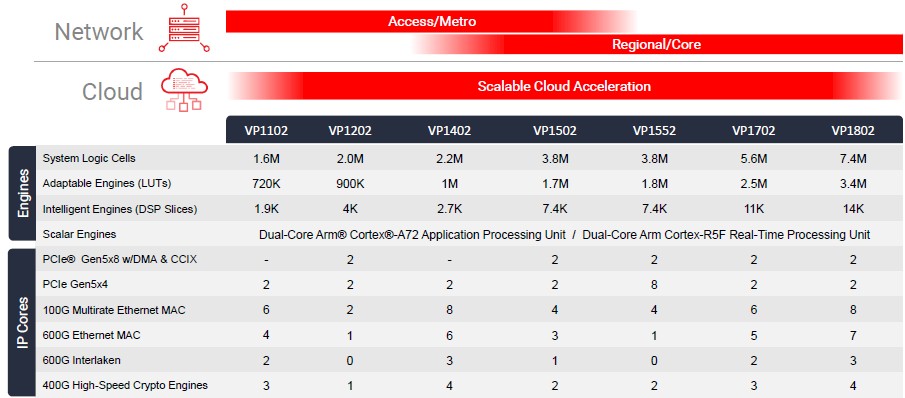
As you can see, Xilinx thinks the middle of the product line is suitable for use in the clouds. The current F1 instance on the Amazon Web Services cloud is a variant of the current Virtex UltraScale+ chip, and it seems likely that AWS will upgrade to Versal Premium variants when they become available. The less beefy versions of the Versal Premium chips on the left side of the table are aimed at metro and access networks and the ones on the right are aimed at regional and core networks. Customers who want to get started on integrating the Versal Premium chips into their systems can get evaluation kits based on the less capable Versal Prime devices and then switch over to the higher-end products once they are available next year. The tools for the Versal Premium devices will be available in the second half of the year with first silicon shipping before June 2021.

Xilinx Works From The Edge Towards Datacenters With Versal FPGA Hybrids
The “Everest” family of hybrid compute engines made by Xilinx, which have lots of programmable logic surrounded by hardened transistor blocks and which are sold under the Versal brand, have been known for so long that we sometimes forget – or can’t believe – that Versal chips are not yet …

Xilinx Benefits From Intel FPGA Shortages
As AMD is getting closer to closing its $35 billion acquisition of FPGA maker Xilinx, it is natural to think about how well that business is doing and how it is competing against its main rival, Intel – specifically, the Programmable Solutions Group, formerly known as the free-standing Altera before …
What Gelsinger Can Do To Unscrew Intel
A little more than a week ago, Intel announced that Pat Gelsinger, its former chief technology officer and former manager of the predecessor of its Data Center Group as well as the current chief executive officer at server virtualization juggernaut VMware, would be returning to the world’s biggest chip maker …
There seem to be a few pieces missing. Having broadband connectivity among FPGAs does not guarantee that there will be no traffic congestion. This condition exists when instantaneous bandwidth generated by one or more FPGAs exceeds the bandwidth available on any of the output ports. Neither Ethernet or Interlaken or even FlexE have the capability to resolve bandwidth oversubscription case. Typically this is handled by switch fabric in a telco-grade (i.e. w/o loss of a single packet) transport network. For data centers, this function usually handled by Top Of the Rack (TOR) switches (e.g. RoCE). Having FEC for error correction has not been very popular in scalable compute because of the long latency of the entire frame vs. just a few bytes of a single RDMA access. Cray, NVIDIA and Intel scalable interconnects all have much smaller payloads for scaling data with “in-flight” error correction other than Ethernet packets and OTN frames. Hopefully, XILINX’s acquisition of SolarFlair and/or internal research efforts will soon shine some light on these missing pieces.