

Companies invest in platforms over a decade or more, and that is why architectures persist longer than we might think given technological differences and economic forces. It is unreasonable to expect a roadmap from any component supplier that spans ten years, but companies do expect to see at least two generations out and then have past performance on the two prior generations to plot a course to the future.
AMD is now at the point in both its Epyc CPU and Radeon Instinct GPU accelerator product lines that it has re-established credibility with its several generations of products and has increasing credibility as we look out into the future with products that are due in 2021 and 2022. Those roadmaps and the path to the future were on display at AMD’s Financial Analysts Day in San Francisco last week. We wanted some time to carefully consider these roadmaps rather than just ricocheting them out to you, and we thought it prudent to talk about the money that was at stake because, ultimately, that is what is going to matter to AMD as it tries to grow its datacenter business. We think there is definitely a path for AMD to get somewhere between 20 percent and 25 percent of datacenter compute spending between now and, say, 2026 or 2027, and we explained our thesis here.
Now, let’s talk about the chip team at AMD, the roadmaps they created, and the nature of the datacenter markets that AMD is chasing with its CPUs and GPUs.
Oddly enough, it all starts with former Lenovo executive Rory Read, who was named chief executive officer of AMD in early 2011. While Lisa Su, who has been chief executive officer at AMD for a little more than five years, deserves a lot of the credit for building the team that has brought AMD back to the datacenter, Read got the ball rolling and Papermaster did two key hires – Jim Keller for CPUs and Raja Koduri for GPUs – that got AMD back in the CPU and GPU games.
Papermaster, who had headed up design of processors at IBM and Apple, joined AMD in the fall of 2011 as chief technology officer, and then shortly thereafter brought in Su, a long-time chip executive at Texas Instruments and IBM Microelectronics, in 2012 to run the business operations of the company. Su notably headed up the project that created the Cell hybrid CPU-GPU processor that underpinned game consoles from Sony; Nintendo used custom PowerPC processors, but not the Cell chip. This was important because that game console business gave AMD some cash flow and engineering chops to steal the business away from IBM, and for several generations now, Sony and Microsoft game consoles are powered by custom AMD CPUs and GPUs. Papermaster hired away Koduri (now at Intel steering Xe discrete graphics development) and Keller (a designer of Alpha RISC processors at DEC, MIPS processors for network devices, Power processors at PA Semi, and Arm processors from Apple) to create its revamped server chip architecture, which we now know as the Epycs. It is debatable if the Graphics Core Next (GCN) design that Koduri championed panned out as well as was hoped, but there is no question that the Epyc architecture, with the Zen cores envisioned by Keller’s chip design team, have revitalized AMD in CPU compute in both PCs and servers.
To get its GPU house in order – which is something that Su & Company very much want to do with Nvidia having the vast majority of GPU accelerator sales in the datacenter for the past decade and with Intel intent on carving out a slice of this market for itself – AMD has brought back David Wang to head up its Radeon Technologies Group. Wang cut his teeth designing graphics processors at supercomputer maker SGI in the 1990s and did a stint making GPUs for Nintendo game machines at the turn of the century before joining ATI Technologies, where he worked on discrete GPU designs and ultimately made them well enough that AMD paid $5.6 billion in 2006 to buy ATI and to take Nvidia on. Wang stayed on at AMD until the summer of 2012, when he left to join AI chip startup Synaptics, where he led chip development for the human interface specialists. Wang Returned to AMD two years ago and has been spearheading the development of the RDNA and CDNA architectures for GPUs that, among other things, have allowed AMD to win both the CPU and GPU compute engine components of the 1.5 exaflops “Frontier” supercomputer to be installed in Oak Ridge National Laboratory in 2021 and the 2 exaflops “El Capitan” supercomputer going into Lawrence Livermore National Laboratory in 2022.
The AMD technical and management bench has gotten wider and deeper over the past decade, and it takes a lot of people to come up with a winning strategy and then execute on it. But we would point out that one other very important hire was Forrest Norrod, who used to run the massive custom server business at Dell and then all of Dell’s enterprise and consumer product engineering and who has been running the Enterprise, Embedded, and Semi-Custom group at AMD since 2014. Norrod has made sure that the engineers working on AMD CPUs and GPUs are making the products that hyperscalers, cloud builders, enterprises, and supercomputing centers will buy. And, as confidence has grown in AMD, buy they have.
The Crown Jewels Of High Performance
For the past five and a half years, the IT industry has been watching AMD very closely, and many have been critical that the company did not push far enough, fast enough. We certainly felt that way in 2015 just after founding The Next Platform, but we were also hopeful that true competition could come to CPUs and GPUs in the datacenter. AMD just had to remember who it was, and what its role was in the industry, and then execute. And that memory and then a new way of executing against it was precisely what Su engineered to happen, step by step, as a good engineer does.
“Why do we love high performance computing so much?” Su asked rhetorically. “We really believe that this is a technology that is the enabler for both the present and the future. It actually drives what can be done over the next number of years. And whether you’re talking about very, very big systems – like supercomputers or the cloud or the hyperscale environments, whether you’re talking about new workloads like big data analytics and visualization – you are talking about the things that we enjoy, like gaming and new client devices. All of these have one thing in common: They all require high performance computing and they really play to our strengths.”
That was how AMD moved into the server space with vigor and success with the Opteron server CPUs in the early 2000s, when Intel left the door wide open between its 32-bit Xeons and 64-bit and largely incompatible Itaniums, and it was how ATI was competing with Nvidia and others in the GPU business since its founding and throughout the time that it was part of AMD.
Everything looks obvious in hindsight, but making big bets takes a certain amount of courage and AMD certainly has shown gumption in the past five years, and it has been on a roll again in the datacenter, re-establishing itself and building credibility. When you boil it all down, it comes down to what Su calls the HPC crown jewels.
“As we formulated our strategy and plans over the last five years, the most important decisions that we had to make and frankly that any technology company has to make is around those technology investments.” Su explained. “It actually takes years to develop a new architecture and to create that foundation to build great products. And when you think about those strategic decisions, they really lead us to where we are today. So these investments include things like our Zen roadmap. With our leadership CPU roadmap, we invested in Zen and it was a big, big performance boost. We’re now with Zen 2, and you are going to hear more about what’s coming. We’re investing in a new graphics architecture with RDNA, and RDNA is actually very unique because it spans consoles, PCs, and even mobile gaming and it will last us again for the next five years. We also made a choice – and this was an important choice – to move our entire product portfolio to 7 nanometer – and very, very aggressively. And that has really paid off for us with now best in class manufacturing. When we saw some of the constraints of Moore’s Law, we said, hey, there’s a different way to do this, there’s a better way to do this, and it involves a chiplet architecture, which allows you to put the best technologies on a package and to some extent break the constraints of Moore’s Law. Now, these things actually may seem pretty obvious today, but frankly, five years ago they weren’t so obvious and they really are the strategic decisions that lead us to today’s product roadmap.”
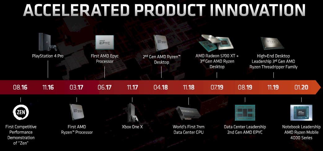
Let’s take the Epyc CPUs first, and there are not a lot of surprises in this roadmap that we don’t already know about.
It is interesting to note that AMD did not talk about Epyc processor roadmaps specifically but rather the evolution of the cores that are used in both the Ryzen PC and Epyc server CPUs. The first generation “Naples” Epyc 7001 processors were based on the Zen1 cores, which had a 51 percent instructions per clock (IPC) boost compared to the prior Dozer family of cores used in the last generation of Opteron processors, which was admittedly a big leap but it was also over a very long timeframe so perhaps not much more than AMD would have gotten if it had stayed in the server racket after 2010 and not walked away as Intel was eating all of its market share gains.
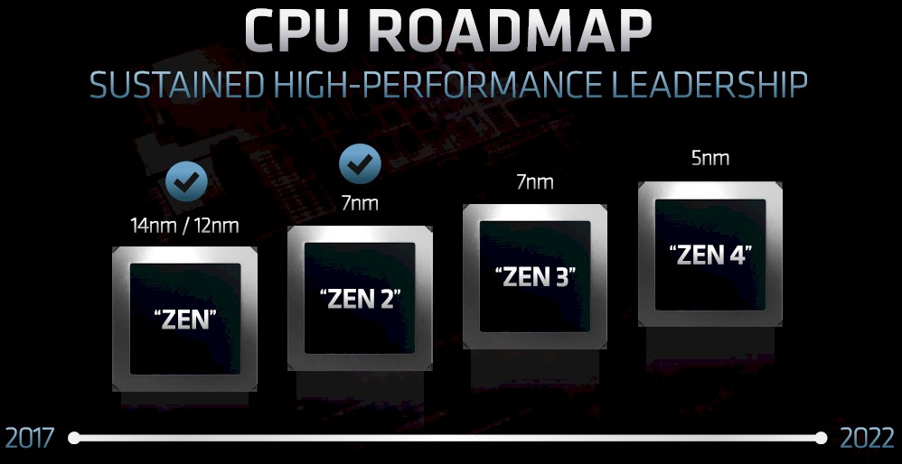
With the Zen 2 cores used in the “Rome” Epyc 7002 processors, the IPC jump was about 15 percent, and the company shrank the CPU cores to a 7 nanometer process and broke them into chiplets surrounding a 12 nanometer I/O and memory hub that actually made the Rome chiplets work better than the Naples ones had. Papermaster, who gave the presentation about the processor architectures, did not talk explicitly about the IPC improvements expected with the Zen 3 core coming with the “Milan” Epyc 7003 processors slated for delivery later this year, but the chatter is that it will be somewhere around 10 percent to integer throughput and somewhere around 50 percent for wider SIMDs on floating point throughput. (Most IPC comparisons are for integer only, and this is certainly true for the figures we have always gotten out of Intel for its Xeon families of server chips.) Papermaster also confirmed that Taiwan Semiconductor Manufacturing Corp, just about everybody’s foundry except Intel and Samsung these days, has rejiggered its process roadmap and that what it had expected to be a significant 7+ nanometer bump has just had its tweaks rolled into the regular 7 nanometer process. We think that this probably means the IPC improvements might be more subdued in Zen 3 than AMD might have been expecting. What we do know from what Papermaster said is that about 40 percent of the improvement in single-threaded performance for the Zen 2 cores compared to the Zen 1+ cores used in the Ryzen PC chips two years ago (based on 12 nanometer processes instead of the 14 nanometer processes used in the Zen 1 cores) was due to 7 nanometer shrink and the clock frequency improvements and the remaining 60 percent was due to straight IPC enhancements. Our point here is that if process comes in a little light with Zen 3 cores, AMD can make it up with a little extra clock.
The other point to make is that AMD will, thanks to TSMC, have process lead for the foreseeable future against rival Intel, which Papermaster was obviously pleased to show:
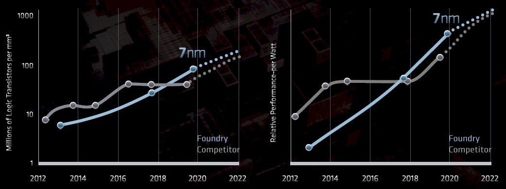
It looks like Intel and TSMC will converge at their respective 5 nanometer processes in 2022, when AMD plans to ship the fourth-generation “Genoa” Epyc 7004 processors. The convergence is not perfect. Intel’s 10 nanometer processes used on the future “Ice Lake” Xeon SPs is roughly analogous to TSMC’s 7 nanometer processes and the 7 nanometer process created by Intel for its future “Sapphire Rapids” Xeon SPs (notably to be used in the 1.3 exaflops “Aurora A21” supercomputer at Argonne National Laboratory) is analogous to the 5 nanometer TSMC process used to create the Genoa Epycs. The naming conventions are deliberately designed to confuse, and the camps of Intel and everybody else accuse the other of being misleading. The future “Graphite Rapids” Xeon SPs expected in 2022 will be using a tweaked 7 nanometer process from Intel, which will be akin to the 5+ nanometer technology from TSMC. Also, there is shifting uses of different processes. There is also chatter that Sapphire Rapids could revert to Intel’s 10 nanometer process (akin to TSMC’s 7 nanometer), and thus the data is a bit fuzzy. Papermaster’s point is that AMD will, as far as anyone can tell, be able to deploy more transistors per unit of area and deliver better inherent performance per watt than Intel in the next three years (inclusive) as it has been able to do since last year with the Rome Epyc chips.
Finally, A Coherent Strategy
CPU design is not just about pipelines and IPC and cores and throughput, of course, and AMD was an innovator with 2.5D HBM (with partners Samsung) for graphics cards back in 2015, and it revamped multichip module packaging for the Ryzen and Epyc lines in 2017. (AMD, like other chip makers, had done multichip packaging a decade ago, here and there, when it was deemed expedient for competitive reasons, and the Opterons were famously MCMs and not monolithic designs.) AMD has innovated with the chiplet design used in the Rome Epycs, which have mixed process resolution, with cores being small and memory controller and I/O functions converged on a lower resolution chip that better matches the power profile of memory and I/O devices. Looking ahead, Papermaster said that AMD was exploring how to use what it called X3D packaging, a mix of 2.5D and true 3D packaging to stack up memory and compute in a package.
Obviously, that Infinity Fabric that connects the chiplets together in the package and then CPUs and GPUs to each other inside a server node is going to play a big part in the architecture of future AMD compute engines.
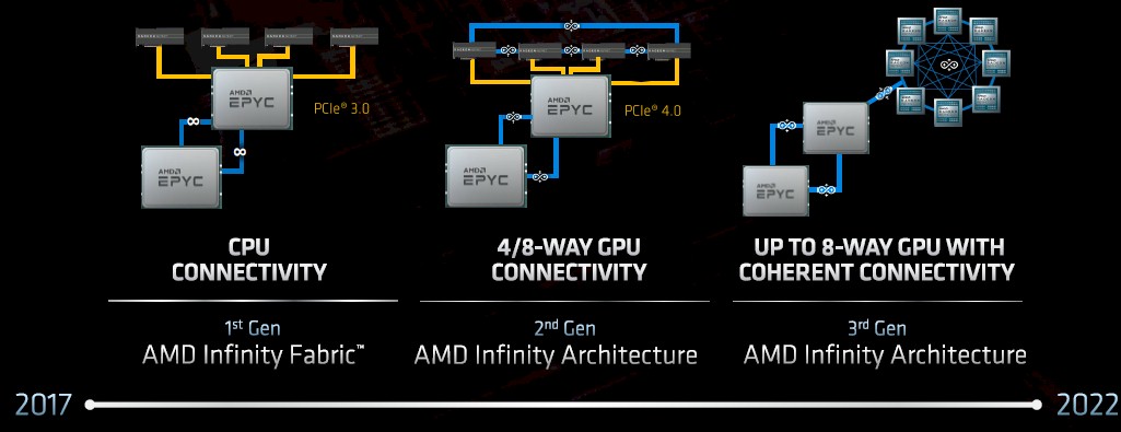
With the initial Naples Epyc processors and early Radeon Instinct GPU accelerators, Infinity Fabric, which was based on the PCI-Express 3.0 protocol, was designed to link the chiplets inside of the CPU socket as well as two CPUs in a NUMA shared memory configuration across a pair of sockets. With the Radeon Instinct MI50 and MI60 GPU accelerators announced in November 2018, the “Vega20” GPUs had a pair of PCI-Express 3.0 ports added to them to allow for up to four GPU cards to have their memories interlinked so they could share data with memory atomics like a pair of CPUs and using the Infinity Fabric 2.0 protocol that is also used by the PCI-Express 4.0 ports on the Rome Epyc chips for NUMA clustering. In the future “Genoa” Epyc processors and the second generation of CDNA (short for Compute DNA) GPUs that are coming for the Radeon Instinct accelerators in the 2021 timeframe, the Infinity Fabric 3.0 protocol, presumably running atop PCI-Express 5.0, will support memory sharing across up to eight Radeon Instinct GPUs as well as across up to a pair of Genoa Epyc CPUs, all in the same memory space.
The Datacenter As A Game Console At Scale
This coherency across the CPUs and GPUs is at the heart of AMD’s ability to be the CPU and GPU motors of choice in the Frontier and El Capitan supercomputers.
IBM has been doing CPU-GPU memory coherency since the Power8’ – that is a prime sign, not an apostrophe, and distinct from a plus sign, which usually meant a process shrink and some microarchitectural tweaks in the Power chip line – shipped in September 2016. It was a bit rudimentary at first, with the Linux kernel having unified but not yet coherent memory access across the Power8’ processor and the “Pascal” Tesla P100 GPU accelerators. But in late 2017, when the Power9 chips started shipping in the “Summit” and “Sierra” supercomputers that IBM was building for the Oak Ridge and Lawrence Livermore labs of the US Department of Energy, the Linux kernel and the Nvidia drivers were tweaked to provide this coherency and, lo and behold, it actually worked.
IBM doesn’t get credit for this, but it created shared memory between processor cores and accelerator cores in the Cell architecture that was used in game consoles and supercomputers ahead of AMD’s own launch of the Heterogeneous System Architecture (HSA) in the early 2010s and its subsequent Accelerated Processing Units, or APUs. IBM tested many of these ideas on the petaflops busting “Roadrunner” supercomputer at Los Alamos National Laboratories, which was built from a pair of AMD Opteron processors and two pairs of IBM Cell coprocessors, all linked over a 20 Gb/sec InfiniBand DDR interconnect. This was not fast enough for memory coherency, but the difficulty in programming the 1.7 petaflops Roadrunner machine demonstrated that faster linked would be needed for coherency as well as a better software environment to manage the compilers across the CPUs and GPUs and their memory use.
These converged CPU-GPU architecture, embodied by AMD in the HSA architecture and its APUs, did not take off commercially in the datacenter – mostly because AMD’s CPUs and GPUs of the time were weaker than the Intel and Nvidia alternatives, respectively. But they sure did take off in the game console market as AMD displaced IBM as the hybrid motor of choice for Microsoft and Sony. (Nintendo went from PowerPC Cell hybrid chips to hybrid Tegra chips from Nvidia.)
What AMD wants to do is stretch its game console approach across racks, rows, and datacenters and it is focusing almost exclusively on hybrid collections of discrete CPUs and discrete GPUs this time around, converged inside of a server, rather than a CPU and a GPU converged inside of a socket. At least for datacenter uses. And this is important because datacenters do not want to have the ratio of CPU and GPU compute locked down inside of a socket because different workloads will require different ratios and, moreover, they want for CPU and GPU compute to be disaggregated and recomposable.
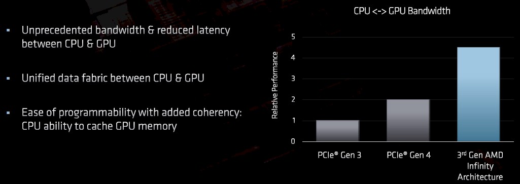
This coherent memory across AMD Epyc CPUs and Radeon Instinct GPUs will give its customers all of the benefits of the NVLink interconnect that IBM and Nvidia created to work atop 20 Gb/sec and then 25 Gb/sec SerDes signaling without having to resort to creating unique communication SerDes on the devices as IBM and Nvidia have had to do. We presume Infinity Fabric 3.0 links will be based on PCI-Express 5.0 transports, at least from the CPU to GPU bandwidth chart that Papermaster showed off:
“And I will tell you that it was a heated competition for these systems,” Papermaster explained, referring to the Frontier and El Capitan machines that helped define and will put to use this coherency, which is part of the current IBM Power9-Nvidia Tesla V100 systems that Oak Ridge and Lawrence Livermore are currently using. “We love the fight at AMD –that is what we’re made of. And so that fight drove us to improve our roadmap, to improve our competitiveness, to go head-to-head and simply beat the competition.”
To Infinity (Fabric) And Beyond
Having competitive CPUs and a competitive interconnect with memory coherency are important in these hybrid systems, but so is having a competitive GPU, which has been a weak spot for AMD for the past decade, particularly with AI and HPC systems and in particular with regard to the software environment that spans the CPUs and the GPUs. This is where Nvidia has been brilliant, of course. It’s Tesla GPU accelerators and CUDA programming environment are the touchstone for HPC and machine learning training. And AMD knows that.
So that is why AMD is going to take a page out of the Nvidia playbook and bifurcate its GPU product line:
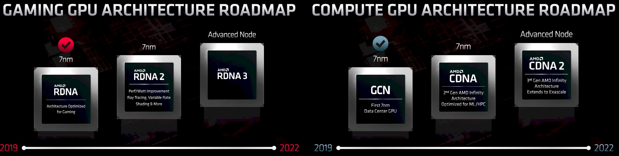
Up until now, AMD has had a single GPU architecture that spanned visualization and graphics on the one end and datacenter compute on the other, and now, with Wang back in charge, the company is creating two distinct products: RDNA aimed at gaming and visualization and CDNA aimed at compute. The details are a little bit thin, but the initial “Navi” 7 nanometer RDNA GPUs, used in the Radeon RX 5700 XT cards, sport a new architecture aimed at gaming that deliver a 50 percent performance bump compared to the prior Vega20 GCN GPUs. About half of that was the move from 14 nanometer to 7 nanometer processes and the other half was a change in architecture such as a much more streamlined graphics pipeline and a multi-level cache hierarchy. With the bump to RDNA2 chips, slated before 2020 for client devices, there will be another 50 percent performance bump as AMD moves to a different manufacturing process node, probably 5 nanometers, but we will see.
AMD is being a bit vague about what will make the CDNA architecture for datacenter compute different from the RDNA architecture for graphics and visualization. “A big part of that CDNA optimization is indeed adding some higher density math for HPC and for what we call tensor ops, the matrix acceleration ops that are needed for HPC and machine learning acceleration,” explained Wang. “And we are optimizing the architecture for compute, so that means we are putting less focus on other operations that are less important for high performance computing.” Wang also called out the need to have coherency across those components because machine learning models were busting out beyond the confines of a single GPU’s memory. This hardware coherency is going to take some time.
So will expanding the use of the Radeon Open Compute (ROCm) development environment, which is the analog to Nvidia’s CUDA environment. But across the $1.2 billion allocated for the Frontier and El Capitan systems, about $220 million of that is for non-recurring engineering (NRE) costs that will largely be focused on making OpenMP and OpenACC play well with ROCm, which is open source. These HPC centers, and presumably more than a few hyperscalers and cloud builders as well as the Cray unit of HPC that is building the systems and their Linux environment for them, will be kicking into the ROCm software work better and scale further than it does. CUDA may be freely distributed, but it is not open source and neither are Nvidia’s drivers – and in the end, couple to better price/performance for both CPU and GPU compute, the openness of the software may have tipped the balance in AMD’s favor.
“As much fun as the last five years have been, today is really about the future, and we like to talk about what we see over the next five years,” Su said. “If you ask me or anybody on this leadership team, we are even more excited about the coming journey in terms of what we can do. And the reason is very simple. First of all, the opportunities are larger. The impact we can make on the industry is larger and our resources are much stronger. And so if you think about those things and what we’ve been able to accomplish, it’s really exciting to think about what we will accomplish. We will stay committed to high performance computing leadership. That is our mantra. We are uniquely very, very good at it. And frankly, there are very few companies in the industry that can possibly do it. It is extraordinarily hard to stay at the bleeding edge.”
One last thing: Isn’t it weird that AMD can do four Epyc CPU processors from 2019 through 2022, inclusive, but can only do three Radeon and Radeon Instinct GPUs in those same four years? The reason, we suspect, is that it is really six GPUs in four years – three for clients and three for servers – and when you look at it that way, you can see the ambition. Besides, all AMD has to do is keep pace with Intel and Nvidia, and they are not on an annual cadence with GPU compute. Yet.

Pushing AI System Cooling To The Limits Without Immersion
Here is a question for you. What is harder to get right now: 1,665 of Nvidia’s “Blackwell” B200 GPU compute engines or 10 megawatts of power for a four year contract in the Northeast region of the United States? Without question, it is the latter, not the former, and both …
The Datacenter GPU Gravy Train That No One Will Derail
We have five decades of very fine-grained analysis of CPU compute engines in the datacenter, and changes come at a steady but glacial pace when it comes to CPU serving. The rise of datacenter GPU compute engines has happened in a very short decade and a half, and yet there …
The AI Wave Finally Starts Lifting Dell And HPE
It is beginning to look like the Dell Technologies and Hewlett Packard Enterprose, the world’s two biggest original equipment manufacturers, are finally going to start benefitting from the generative AI wave, mainly because they are finally getting enough allocations of GPUs from Nvidia and AMD that they can start addressing …
With regards to GPU cadence, it is also worth noting the 2 custom designs for the forthcoming Sony and Microsoft consoles – those must have kept engineering resources focused…
Nintendo used Cell CPUs? Can you cite a source for that?
Brain fart. Nintendo used the custom “Broadway” and “Espresso” PowerPC processors from IBM in its game consoles, but not a full blown Cell chip.