

The European Exascale Processor Memory Node Design (ExaNoDe) project has wrapped up, delivering a prototype multi-chip-module (MCM) that integrates Arm cores, FPGAs, and 3D active interposer/chiplet technology.
The primary goal of the three-year, €8.6 million effort – which we first profiled back in August 2016 – was to develop the architectural foundations of a compute node suitable for exascale number-crunching. ExaNoDe is one of four projects being funded out the European Union’s Horizon 2020 program that is funneling into the larger European effort to design and build a fleet of exascale supercomputers in the next decade.
To dig a little deeper into what the prototype system entails and how the technology will move forward in the EU’s exascale plans, we spoke with Denis Dutoit, who led the effort as the ExaNoDe project coordinator. Dutoit’s day job is a research engineer at CEA-Leti, where he works in the chip architecture and design group. That background, plus fact the CEA-Leti is the coordinating organization in the 13-partner ExaNoDe consortium, landed him the role as the project lead.
According to Dutoit, the main focus of the ExaNoDe work was to integrate the various processor and memory technologies of interest to the Europeans into a package that could serve as the basis for an exascale node. Prime drivers in the design were energy efficiency and cost. To the extent possible, these technologies are based on intellectual property that were developed (or could be developed) within the EU, thus the emphasis on Arm, FPGAs, and custom-built chiplets.
As pictured below, the node prototype board is comprised a pair of MCMs, each with two FGPAs. The MCM on the left has an interposer topped with what appears to be three chiplets. Dutoit says the FPGAs are the same ones recently delivered in the ExaNeSt project prototype, namely the Xilinx Zynq Ultrascale+ SoCs. Embedded in these SoCs are Arm Cortex-A53 cores, which serves as the Arm component here.
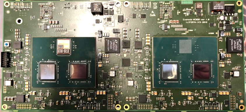
The motivation to employ the same FPGA hardware was to be able to reuse the same software componentry across the projects. Dutoit says that in a production version of the exascale node, “the aim is to have the Arm cores inside the chiplet,” the rationale being to put the general-purpose compute hardware as close as possible to any special-purpose accelerators on the chiplet in order to save energy and shorten the communication path.
The chiplets delivered with the prototype, which were manufactured by STMicroelectronics’s FD-SOI 28nm process, only contain communication logic for the interposer-chiplet complex plus a specialized hardware block for accelerating convolution neural network (CNN) computations. In this case, the CNN accelerator, which is based on an open-source implementation (EvaConv) developed at ETH Zurich, is only for demonstration purposes, although it would certainly be a prime candidate to include in a production chiplet, given the interest by HPC users to apply deep learning to their application workflows.
Because of the large size of the FPGAs, these devices are likely to remain as distinct components on the MCM going forward, Dutoit says. Their purpose is to serve as a platform for specialized application functions that don’t warrant the development of a hard-wired custom chiplet.
The memory components in the prototype are external to both the interposer and the MCM. In a production implementation, the intention is to have high bandwidth memory (HBM) stacked on the interposer right next to the Arm chiplets and any special-purpose accelerators, again the idea being to shorten the data path and conserve energy.
The ExaNoDe memory system is based on UNIMEM, a PGAS-style global addressing scheme that allows compute nodes to share non-coherent memory across a cluster. Essentially, it’s a model that separates local coherent memory with that of remote memory, employing an API to negotiate between them. Underneath the covers, it uses RDMA to provide access to data where it resides, largely avoiding costly copies between nodes. UNIMEM was developed by the EUROSERVER project, yet another EU initiative aimed at developing domestic computing IP.
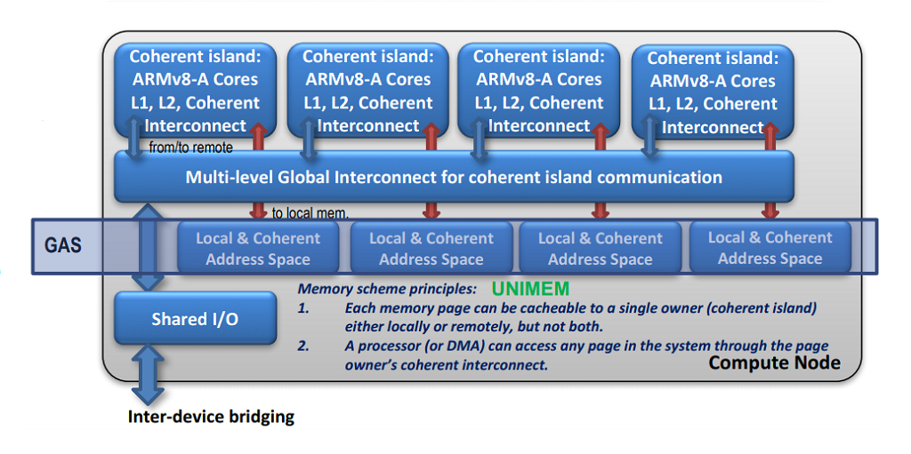
One of the other home-grown technologies that made it into the prototype was the active interposer, which had been developed by CEA-Leti in an unrelated project under separate funding. The base interposer was manufactured by STMicroelectronics, while the thru-silicon via (TSV) and microbumps integration was done in CEA-Leti’s own fab. The interposer/chiplet complex, which the project refers to as a “3DIC,” represents ExaNoDe’s major contribution to the larger exascale effort underway on the continent.
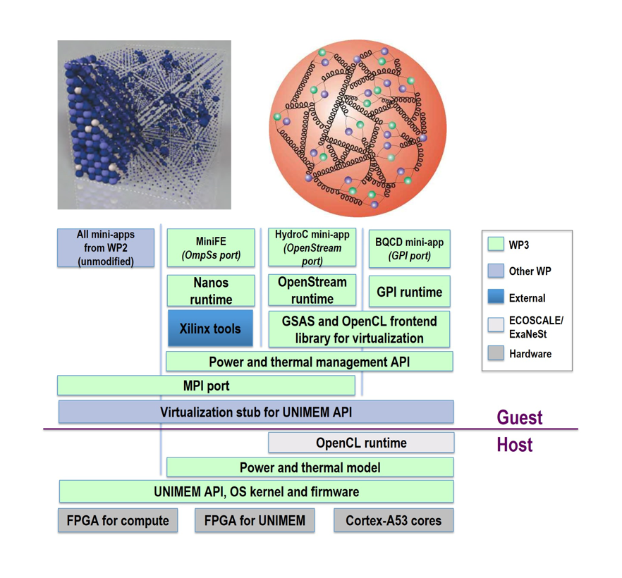
On the software side, four HPC applications have been ported to the prototype as a demonstration of how such workloads can be accelerated on a heterogeneous node. They include BCQD, a lattice quantum chromodynamics simulation code; HydroC, a simplified version of the astrophysical code RAMSES; miniDDR, a materials science application based on KKRnano, and miniFE, a finite element generation, assembly and solution for an unstructured grid problem. The compute node’s FPGAs were specifically used to accelerate the kernels of these mini-applications. The diagram below illustrates how these applications ride on top of the software stack that has been stitched together for the ExaNoDe platform.
Dutoit tells us that going forward, the ExaNoDe software building blocks and application ports will be taken up by EuroEXA, a project tasked to design and build a petascale prototype using FPGAs, Arm, and other technologies. Meanwhile, the hardware work will be passed off to the European Processor Initiative (EPI), an EU project to develop a domestic HPC chip for pre-exascale and exascale supercomputers. “All the we have learned from 3D integration, chiplet partitioning, and methodologies for this kind of technology will be the basis for the EPI processor,” says Dutoit.

German HPC Center Is The First Buyer For New D-Wave Quantum Computer
The quantum computing space is replete with big-name companies like IBM, Google, Microsoft, Amazon, and Intel touting incremental but important steps they’re taking to bring the long-promised technology to the fore. Most recently, Google in December announced that, with the introduction of “Willow” chip, its scientists in its Quantum Lab …

A Status Check on Global Exascale Ambitions
As we head toward the annual Supercomputing Conference season we wanted to take a moment for a level-set on exascale. There has been much talk about reaching this pinnacle over the last several years and while plenty of centers say they have reached exascale, that is only for single-precision peak …
European Processor Initiative Readies Prototype
Europe is trailing the other major HPC powers in its quest to field exascale supercomputers. The first such European Union machines aren’t scheduled to come online until 2023, at which point the United States, China, and maybe even Japan are likely to have their initial systems up and running. But …
Be the first to comment