
It is going to take a lot of different things to build an exascale system. One of them is money, and the other is a lot of good – and perhaps unconventional – ideas. It may also take more cooperation between the hyperscale and HPC communities, who both stand to benefit from the innovation.
As a professor of computer architectures at the University of Manchester, the director of technology and systems at chip designer ARM, and the founder of a company called Kaleao to create microservers that implement many of his architectural ideas, John Goodacre has some strong opinions about how to get to exascale class systems in a timely fashion and in a way that is not going to require the power of many nuclear reactors.
Goodacre’s original target was hyperscale workloads, but what applies to hyperscalers applies equally well to high performance computing, and he explained as much in a session at the ISC16 supercomputing conference. And he explained that it would take a holistic approach – with advances in the memory hierarchy to the operating system kernels and runtimes to the interconnect and system packaging – to come even close to getting an exascale system into the field in 2020 or so that is within a reasonable power envelope and that has enough main memory capacity and computing oomph to do more than run the Linpack benchmark test.
The work that Goodacre and his team have done, which are being commercialized by Kaleao, are being advanced and tweaked for the HPC space under the auspices of the European Horizon 2020 program, which is a massive €80 billion effort spanning 2014 through 2020 to spur research and innovation in all kinds of fields relevant to the competitiveness of Europe in the global economy.
The extension of the webscale architecture embodied in the various projects that are being commercialized by Kaleao into HPC is not just a reach for a new market, but inevitable. Goodacre believes that many of the key technologies developed to parallelize supercomputing applications – including the Message Passing Interface (MPI) protocol for sharing work across a cluster and the Partitioned Global Address Space (PGAS) memory addressing scheme – will have to be integrated into the programming model of a future exascale system no matter what workloads they run. This will be the only way to make use of the millions of threads in the system in such a way as to be compatible with existing applications, and new applications can benefit from the architecture as well. This is something that is lost on hyperscalers today, who have their own means of creating massively distributed applications. Perhaps running such applications on a Java substrate is not the most efficient use of compute, networking, and storage, even if it does ease the programming a bit, but the hyperscalers are rich enough that they don’t have to care.
For now.
The lynchpin of the unifying exascale effort that Goodacre and others have proposed to the European Union for funding is the EuroServer project, which culminated in a system architecture being commercialized by Kaleao that uses ARM-based processors for compute and includes integrated memory, flash, and networking on a single system board to reduce the distances between these components and therefore their energy consumption. Here is what the EuroServer, which was announced in November 2014 and which is prototyping now, looks like:
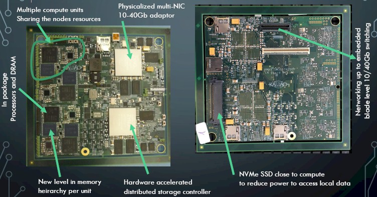
This is a hardware testbed for the scale out architecture Goodacre is proposing, and one that can be put to practical use today by hyperscalers if they so choose. The EuroServer node has four eight-core hybrid ARMv8 processors that implement the so-called big.LITTLE architecture. (Yes, that hurt to type.) With this architecture, you put a mix of wimpy and brawny cores on a single chip so they can do different kinds of work at the most efficient level as possible. In this case, the chip used in the EuroServer has four ARM Cortex-A57 nodes running at 2.1 GHz (those are the brawny ones) and four Cortex-A53 cores running at 1.5 GHz (those are the wimpy ones). Each of these server cards has 4 GB of memory and 128 GB of flash soldered onto them and shared by the four processor sockets; they also share an integrated 40 Gb/sec Ethernet network interface that can be diced and sliced into four virtual 10 Gb/sec ports. Each server is a socket, each card has four sockets, four cards are put onto a EuroServer blade, and a dozen blades fit into a 3U server enclosure. That yields 192 GB of main memory and 6 TB of flash memory in a chassis with 1,536 cores and an aggregate of 960 Gb/sec of bandwidth into the network.
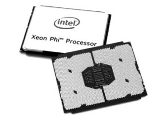
Goodacre and other researchers across Europe are proposing a much denser level of compute, which includes ARM processors as well as FPGAs and high bandwidth memory under a project called ExaNode, which will put blocks of compute and memory on a silicon interposer in a way that resembles the integration of memory and processing on a single package that is employed with Intel’s “Knights Landing” Xeon Phi processors, with Nvidia’s “Pascal” Tesla P100 coprocessors, with Fujitsu’s Sparc64-XIfx processors, and with AMD’s current graphics cards and future hybrid CPU-GPU cards. The ExaNode project has received €8.4 million in funding, and has ARM, Atos/Bull, Kalray, and various institutions including Goodacre’s University of Manchester, the Barcelona Supercomputing Center, Forschungszentrum Jülich, CEA, and ETH Zurich participating to make an ARM-based, accelerated computing element that can rival these parts mentioned above.
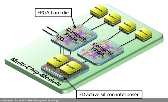
The ExaNode shown in this diagram is but one of several possible configurations. The chiplet is based on ARM cores, and the auxiliary compute can easily be a GPU instead of an FPGA. The number of each type of compute elements as well as the capacity of the high bandwidth memory can be altered as well – integration technology and economics allowing, of course.
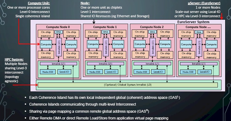
While the hardware integration is important, the neat bit is that Goodacre is proposing a hybrid memory model called Unimem that was developed under the auspices of the separate EcoScale project and that is part and parcel of the EuroServer design.
“The Unimem page is the best of both DRAM memory and other I/O devices, and it sits between the two,” Goodacre explained. “We take away the caching on the local node and leave it on the remote node and be coherent when we access that remote data. That allows something like a direct memory access to go from coherent region to coherent region between two nodes without actually touching a device explicitly in the transfer protocols.”
The combination of Unimem, as well as the use of PGAS to share memory on compute elements and MPI to share memory across compute elements, and the ExaNode architecture is what is going to allow for the dense packaging and high thread count needed for an exascale system, says Goodacre.
“Unlike a processor that traditionally has just a single bus that connects to devices or local shared memory, this allows another device access into that cache hierarchy remotely so that you can start scaling up the global view of the memory on each of the processors while computing locally,” Goodacre explained. “It is actually processor agnostic as long as they can provide this Unimem memory type and you can have heterogeneity both between the units of compute and across them. The key thing is the memory spaces, which include the local one that you have full, SMP-type memory and the remote one that you can access through another compute unit’s cache hierarchy to give you a global view of an additional address space.”
Once you have that compute unit that has the Unimem architecture, you can connect them into a global network. “You have the ability basically to share global address pointers globally across all of the machines, and obviously you are going to put very large pages in such things,” Goodacre continued. “The other way to look at that memory is that it is actually a globally addressable PGAS.”
The neat thing about the Unimem architecture is that it will allow for remote page borrowing, which will allow a processor on one ExaNode to borrow the memory from another with similar latencies as the local memory (so long as these ExaNodes are reasonably close together). Beyond that, the system will be able to create NUMA islands on the fly within the system for tighter coherency, and the system will obviously support loosely coupled architectures common in HPC and hyperscale, too.
The shared resources, like flash memory on the nodes, live in the secondary address space and are accessed natively and without virtualization overhead, says Goodacre. “The storage is converged into the compute, and the memory is converged into the processing devices, and this is very much a hyperconverged approach. Keep everything within that distance. Remember it is 5 megawatts for every word you transmit 5 millimeters using today’s conductors for exascale.”
The nodes need to be linked together to form a cluster, and Goodacre is working with others on yet another project called ExaNest that is creating an interconnect that will have 160 Gb/sec of compute for a server node with four compute units. This ExaNest work is leveraging earlier research on interconnects from the Encore project, which created a 3D torus interconnect for hyperscale applications. The exact dimensions of the topology that Goodacre will propose for an exascale system is still being worked out, but he says the research board has ten 16 Gb/sec links with “quite a good fan out going there” and that they will back down to the level that makes sense depending on how the system is being used.
That leaves software, which is always a pain in the neck for a system architect trying to create something elegant and new.
“Given the huge investment in software, you can’t just leave that behind with a brand new paradigm from Day One,” Goodacre conceded. “So what we are doing is we are mapping most of the existing tools and runtimes onto this new paradigm and then, maybe an Olympic period later, the software will move over and we will start using the new hardware capabilities.”
As for the programming model, the stack will support a modified OpenCL to talk to the various compute elements and employ a mix of NUMA, MPI, and PGAS. “If you look at the way people are partitioning with MPI communication today, we think we can bring the shared memory into the lower level and within that be partitioned into multi-socketed NUMA machines where we are sharing resources much more simply across them.”
So here is the fun bit. Does all of this work get us to an exascale system within a reasonable power envelope? Goodacre says it can with a bunch of qualifications.
“You have got to make some assumptions. We do have some universities working in the optical switch area that believe we can get a 200-rack level switch working at optical. So let’s assume that is going to be our rack limit as well. And it has to have an efficient way to share a global space, and that is quite a big assumption, too, but not impossible. Then the proposed architecture, if you assume around 10 flops per byte at least, we reckon that this architecture with today’s components is 60 megawatts to 70 megawatts at exascale, assuming that you are just working with a few gigabytes of on-chip memory that is really close to the processor. You are easily over 100 megawatts to 200 megawatts by the time you actually hit the capacities of any large application. Counting optimizations that we are looking at today can probably shave off 5 percent or so. After that, it becomes crystal ball. To get it lower, we have got to change that ratio of bytes per flop. The model that we are using memory to store and forward values has to somehow be reduced, whether it is a different programming paradigm – I think data flow is quite an interesting one, especially if you tie that into some sort of microarchitecture to make intermediate values flow without having to go back to main memory – that is all very good.”
The key is to get a better balance between the flops of compute and the bytes of memory and their bandwidth. The best DDR4 memory today burns around 100 picojoules per byte transmitted, so even if you assume you can get that down to 50 picojoules per byte, that is still 50 megawatts at a 1 flop per byte ratio and well above the 25 megawatt envelope everyone was shooting for. (And we think it is more like 40 megawatts these days.)

You can’t trim the main memory back too far because certain HPC applications such as weather modeling, fluid dynamics, structural dynamics, and particle physics, actually require at least 1 flop per byte.
So this, says Goodacre, means the programming paradigm has to change, as he mentioned above. We also need better conducting materials for chips and interconnects, he says.
“Anybody from materials land, we would love anything that conducts better than today’s copper,” he said with a laugh. “A tenfold increase should do nicely, and I don’t think it is optical unless your lasers can run at 100X lower energy. So you really need to find a way to get that less than 30 or 40 centimeters much more efficient so you can get rid of that 5 megawatts per few gigabytes that you need.”
With power companies looking at carbon nanotubes impregnated with various materials for future long-range transmission wires, there is a chance to piggyback on their research. Power companies lose around 50 percent of the electricity they transmit to the heat caused by resistance in the copper wires that are used to make the power grid. The question is whether whatever they come up with can be scaled down and work on a flex cable – and if they can create it in time. It might take until 2024 to accomplish this, Goodacre says.
“If you do all those things, you might just hit that 40 megawatt limit for exascale, and it is more like 50 megawatts. Anything more than that and you will need materials changes in either the processor or a way to run as a superconductor.”

Knights Landing Will Waterfall Down From On High
With the general availability of the “Knights Landing” Xeon Phi many core processors from Intel last month, some of the largest supercomputing labs on the planet are getting their first taste of what the future style of high performance computing could look like for the rest of us. We are …
Competition Heats Up In Cluster Interconnects
Any time a ranking of a technology is put together, that ranking is always called into question as to whether or not it is representative of reality. Rankings, such as the Top 500 list of the top supercomputers in the world, has been the subject of such debate with regards …

Supercomputing’s Scramble to Keep Thinking in Parallel
As supercomputing centers look to future exascale systems, among the other pressing concerns (power consumption in particular) is adopting the right programming approach to scale applications across millions of cores. And while this might sound like a big enough challenge on its own, it gets more complicated because it might …
AMD has a patent pending for adding some FPGA compute to the HBM stacks to go along with the DRAM dies. So maybe an AMD K12 custom ARMv8A ISA running APU that could fit on an active silicon interposer with the FPGA not taking up any extra footprint on the interposer but what the HBM2 dies already take up. JEDEC and Micron as well as Samsung, SK Hynix, and the rest of the HBM industry should try and draft an HBM/NVM standard that uses an NVM(XPoint) die added to the HBM2 stacks, and wired up by TSVs, for an even better HBM/NVM mash-up on the HBM2 stacks solution for some very power efficient distributed in HBM memory FPGA compute, as well as XPoint NVM storage right on the HBM2 stacks.
AMD should be able to get even more of its custom K12 ARM cores on any 14nm process node if it uses its high density designs libraries to tape out a K12 core at 14nm/10nm, and AMD got about a 30% space savings with its x86 Carrizo cores using those high density design layout libraries with Carrizo’s cores at 28nm and without having to go to a smaller process node to get that 30%. Some of those AMD Zen/Vega APUs on an interposer exascale design proposals could just as well be some K12/Vega APU on an interposer designs with FPGA and NVM/XPoint added to the HBM2 stacks, and the power savings would be manifold with both HBM2’s low memory clocks and high effective bandwidth saving power, and NVM/XPoint right near the memory and very accessible to the FPGA in HBM memory compute. This is what exascale computing is very concerned with that extra power savings by not having the compute too far away from the memory, or NVM data stores for the large data sets need for some exascale compute workloads.
Funny is though that AMD has become extremely silent on their K12 it hasn’t been mentioned anywhere recently by any one higher up in the AMD hierarchy. Makes me wonder if they silently abandoned it to focus on Zen instead. Too many eggs in a basket for a resource strained company like AMD usually not a good idea.