

The European Exascale System InterconNect and Storage (ExaNeSt) project has wrapped up, having completed development of its prototype system and run a series of application benchmarks on it. The verdict? According to the ExaNeSt developers, the prototype demonstrates superior energy efficiency on a number of codes and, in at least one case, outperforms a GPU-accelerated system.
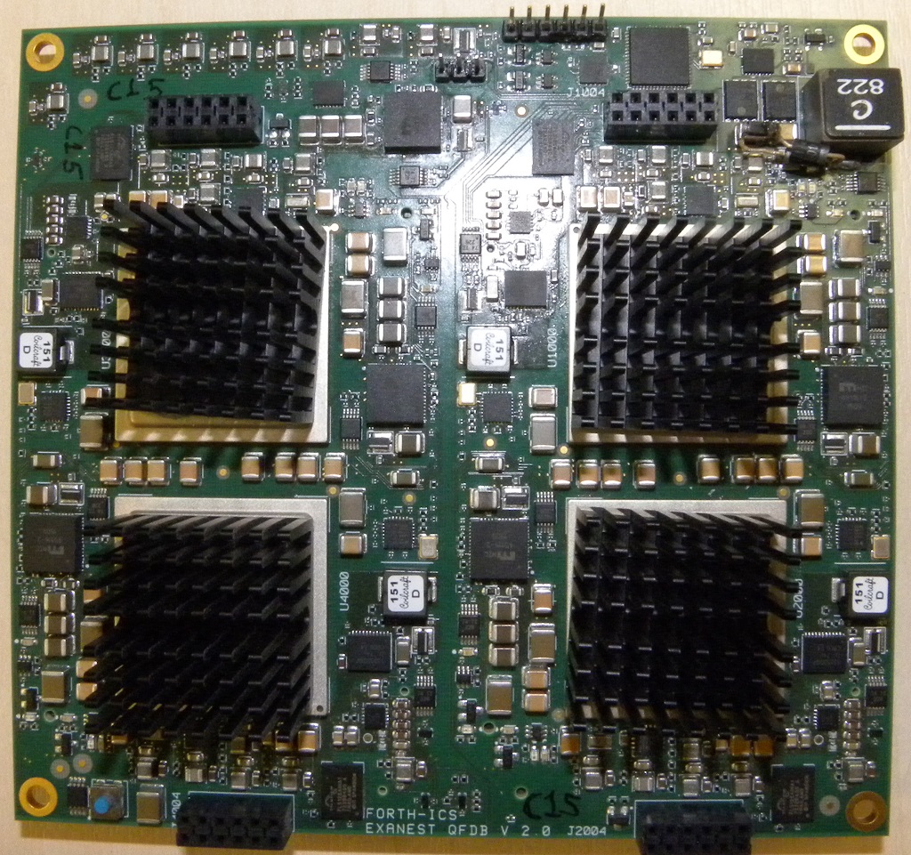
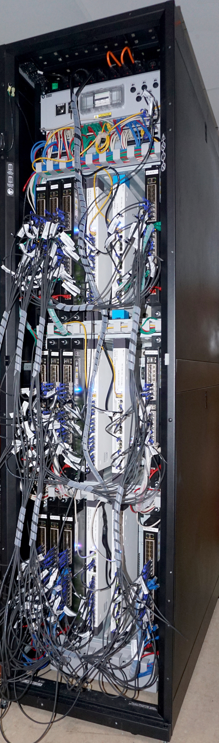
As we reported previously, the ExaNeSt hardware is powered by Xilinx Zynq Ultrascale FPGAs, each of which integrates four 64-bit Arm (A53) cores. Each blade is equipped with four of these FPGAs mounted in a daughter card, as well as 64 GB of DRAM and 250 GB of flash in the form of an SSD. The entire system is made up of 12 of these blades, representing 192 FPGA-powered nodes.
The system interconnect is a rather interesting piece of engineering, inasmuch it’s the only custom component in ExaNeSt. It supports user-level, zero-copy transfers, which is designed to obviate the need for things like caches and kernel buffers. The interconnect links each FPGA in a 3D torus configuration, but is limited to communication within a rack. A multi-rack system, which is just a theoretical construct at this point, would have to rely on a conventional interconnect, such as Ethernet or InfiniBand.
There is no need for network adapters in the prototype since the FPGA itself implements the network router and interface, occupying 40 percent of its programmable logic. FPGA-to-FPGA latency is on the order of 70 nanoseconds, with 155 nanoseconds per hop. Bandwidth is 100 Gb/sec, divided between ten 10 Gbps full duplex links. An optical switch chip was begin developed to enable intra-rack networking, but this component was not completed in time for the final prototype.
Applications tested on the ExaNeSt machine include those in material science (LAMMPS and MiniMD), climate forecasting (REGCM), CFD (OpenFOAM, and SailFish), neuroscience (DPSNN), astrophysics (GADGET, PINOCCHIO, and ExaHiNbody), and data analytics (MonetCB). In most cases, only the Arm cores were used to run these applications, since it takes a good deal of work to port even portions of these codes into reconfigurable logic. That’s unfortunate since each Zynq FPGA contains 10K DSP slices and 2.4 million logic elements, which represent more floating point performance than the four rather measily Arm cores integrated on the chip.
Nevertheless, the ExaNeSt prototype, even using just the Arm component, is quite energy efficient, at least in terms of the energy-delay product (EDP) metric, a measurement that looks at both economizing on energy and reaching the solution fast. For example, running GADGET on 16 of the Arm cores delivered a 16X better EDP than on a 40-core, 2016-era Intel cluster, even as the Arm implementation ran three times slower.
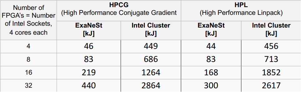
Likewise, when they ran the High Performance Linpack (HPL) and the High Performance Conjugate Gradient (HPCG) benchmarks on the Arm cores, they found the energy used was 6X to 10X less than with the Intel cluster, even though the X86 cluster’s execution was significantly faster.
For the ExaHiNBody code, the Arm solution was not only 12X slower than the Intel cluster, but also used 1.3X more energy. However, when a hand-crafted FGPA implementation for this code was developed, it ran twice as fast as on Intel processors and six times faster than on an Nvidia GTX1080 (Pascal generation). Here, the ExaNeSt protype’s energy efficiency really shined, with a 600x EDP advantage over the Intel chips and 10X better EDP than the GTX1080. In this case, it was even twice as energy efficient as the state-of-the-art V100 GPU.
FPGAs will not uniformly outperform GPUs though. According to ExaNeSt Project Coordinator Manolis Katevenis, GPUs have superior memory bandwidth compared to FPGAs, so they tend to be competitive mostly for compute-bound problems. “FPGAs aren’t the solutions for everything,” he admitted.
And even though the Arm processor cores used in the prototype don’t provide the performance of a modern x86 CPU, Manolis thinks there is untapped potential there. He recounted the history of the x86 architecture, which until the late 1980s was used for low-end chips in personal computers. But the presence of the PC mass market enabled it to be developed into a competitive platform for servers, which subsequently came to dominate the datacenter market all the way up to HPC. He believes the same dynamic may be happening today with Arm, which is the current architecture for the mass market of smartphones and other hand-held devices.
Whether history repeats itself in this instance remains to be seen. It’s doubtful that the HPC community would embrace a new architecture unless it demonstrates both superior energy efficiency and superior performance. (If HPC users thought energy use was more important than performance, they would be purchasing slower processors.) The Scalable Vector Extension (SVE) of the ARMv8 line may be the way to get to better performance, but the technology will have to be embraced by more chipmakers than just Fujitsu.
In the meantime, much of the ExaNeSt work, along with the complementary technology developed in the ExaNoDe and EcoScale projects, will be taken up by the EuroEXA project, which is primarily focused on developing an FPGA-based platform for exascale computing. Manolis told us that EuroEXA will perform more application porting for the current ExaNeSt prototyoe and eventually build what amounts to a second-generation machine. Some of the ExaNeST work, especially around the Arm component, will also flow into the European Processor Initiative (EPI), a project that is developing Arm and RISC-V-based HPC processors for European supercomputers. These will eventually see the light of day in deployed exascale supercomputers sometime in the early years of the next decade. At least that’s the plan.

wow. beat up a Haswell based system and GTX1080, color me unimpressed.
Yeah, IDK. If it were running the codes on the FPGAs then it’d be something to write home about.
I think on the face of it, the fact the system couldn’t be configured easily / in time to run other tests, is why GPUs / readily programmable, will continue to be more advantageous. Hardware moves fast, and software even faster. ‘need to keep up…
This is not true in general. In contrast to current so-called-AI hype with its dynamics for important HPC workloads algorithmic development is actually quite slow. For example in Molecular Dynamics Simulation there are only certain algorithms which are accepted from science side. New algorithms here need many years to get approval. Or take BSIM-CMG which is the standard device model for FinFET transistors, it’s being stable since nearly 4 yrs.
That means that effort in these areas might be good invest.
What I like in this work is FPGA taking NIC role a la Microsoft Catapult, but it would be much more interesting if complete applications would be ported to FPGA and it all comes together. But this is tremendous effort and productivity is orders below CUDA. However there is more to gain here than with GPUs. No free lunch.