

The competition for the compute engines in hybrid HPC and AI supercomputer systems is heating up, and it is beginning to look a bit like back to the future with Cray on the rise and AMD also revitalized.
Nothing is better proof of confidence in the future AMD CPU and GPU roadmaps and the homegrown “Slingshot” interconnect and the “Shasta” systems design of Cray than the fact that these two vendors have just partnered to take down the “Frontier” exascale system to be installed at Oak Ridge National Laboratory as the successor to the current “Summit” pre-exascale system built by IBM in conjunction with GPU maker Nvidia and InfiniBand switch maker Mellanox Technologies.
Nvidia’s sudden desire back in March to shell out $6.9 billion to acquire Mellanox now makes a little bit more sense.
The Frontier system, to be installed in 2021, is part of the CORAL-2 procurement from the US Department of Energy, which is putting exascale systems into Oak Ridge as well as in Argonne National Laboratory – in that case the “Aurora A21” system using Intel Xeon CPUs and Xe GPU accelerators in a Cray Shasta system with Cray’s Slingshot interconnect between the nodes – and in Lawrence Livermore National Laboratory, home to the “Sierra” system that, like Summit at Oak Ridge, is based on the combination of IBM’s “Nimbus” Power9 processors, Nvidia “Volta” Tesla GPU accelerators, and Mellanox 100 Gb/sec EDR InfiniBand networks. Lawrence Livermore has yet to announce the winning bid for its CORAL-2 system, but we strongly suspect that the DOE will want to spread the money around, and its risk, and award IBM the contract to build its “El Capitan” follow-on to Sierra, using Big Blue’s Power10 processors as well as future GPU accelerators from Nvidia and future interconnects from Mellanox. We talked about the $1.8 billion that the US government is ponying up for exascale systems a year ago, and not much was known at the time about Aurora A21 (the successor to the failed pre-exascale machine based on Intel’s “Knights Hill” many-core processors and Omni-Path 200 interconnect that never saw the light of day and that was supposed to be installed last year), Frontier, or El Capitan.
With the announcement of the CORAL-2 machine at Oak Ridge to Cray, which is the prime contractor as the system maker, not the chip maker, should be, we are learning a little more about how the Frontier supercomputer will be built and the value of co-design.
In a press conference previewing the CORAL-2 award to Cray and AMD for Frontier, Pete Ungaro, Cray’s chief executive officer, said that the Frontier system would be comprised of more than 100 cabinets of machinery and would deliver in excess of 1.5 exaflops of raw double precision floating point math capability. Considering that a system architecture generally scales to 200 cabinets at Cray, that seems to imply that it could, in theory, build a 3 exaflops system if someone wanted to pay for it. To give Frontier some physicality, Ungaro said that the machine will be about the size of two basketball courts, will weigh more than 1 million pounds, and will have more than 90 miles of cabling.
Three things are immediately astounding about the Frontier system that Cray is building with the substantial assistance of AMD. The first is that the Shasta racks in the Frontier system will be able to deliver up 300 kilowatts of power density per cabinet. It doesn’t take a supercomputer to figure out that this is a liquid-cooled Shasta system, and even if this is not using a standard 19-inch rack (as we think it will not be), Frontier is going to be setting a very high bar for compute density all the same. Hyperscale datacenters can do maybe 15 kilowatts to 30 kilowatts, by comparison. That compute density in Frontier is being enabled in part by a new heterogeneous CPU-GPU blade design that Cray and AMD worked on together. Frontier will be sitting in a 40 megawatt power envelope, which is about half of what five years ago everyone was worrying an exascale system might consume.
People are clever, aren’t they? That’s why we keep them around. . . .
The second thing that is striking about Frontier is that AMD ran the compute table completely, winning the deal for both the CPU and the GPU accelerators. Given that Thomas Zacharia, director of Oak Ridge, was bragging that the current Summit system built by IBM was completed nine months ahead of schedule and $30 million lower than its anticipated budget way back when the CORAL-1 contracts were bid, and given that IBM and Nvidia did a very good job helping the scientists working at or with Oak Ridge get their codes ported from Titan to Summit, you would have thought that Frontier would almost assuredly be comprised of IBM’s future Power10 processors and a future Nvidia GPU accelerator. But that didn’t happen, and we can only infer as to why this is the case.
This win appears to be about performance and price/performance.
Everyone was expecting Frontier to crest above 1 exaflops at double precision, and very few people had been thinking that with an expected budget of between $400 million and $600 million for exascale systems that the costs would not go right up to the top of that budget. But nonetheless, promising in excess of 1.5 exaflops even at the top end of budget range – $500 million for the Frontier system itself and $100 million in non-recurring engineering (NRE) costs relating to the development of compute, storage, networking, and software technologies that makes the Frontier machine a true system – was more than many expected. AMD is coming through with bang for the buck, which historically speaking, is precisely AMD’s job.
Welcome back, AMD.
As we have pointed out before with the Summit system, the GPU accelerators, which deliver the bulk of the raw compute in the machine, also dominate the cost of the machine. This is reasonable since, in this case, the Nvidia Volta Tesla GPU accelerators are among the most dense and sophisticated computing devices ever invented, with a huge GPU, high bandwidth stacked memory, and packaging to bring it all together. But AMD knows how to make GPU cards with HBM, too, and it has apparently cooked up a future GPU that can do the heavy lifting that both traditional HPC simulation and modeling and new-fangled AI workloads both require – and at relatively compelling price.
“When Nvidia was the only game in town, they could charge a premium price for their accelerators,” Jeff Nichols, associate laboratory director for Computing and Computational Sciences at Oak Ridge, tells The Next Platform, putting it extremely delicately. “The high bandwidth memory and the accelerator costs dominate the costs of these systems.”
That has, without a doubt, not changed with the Frontier machine. But AMD seems to have pushed the envelope on price/performance. We were expecting Frontier to come in at 1.3 exaflops double precision at a $500 million budget when we did some prognosticating a year ago, which was about $385 per teraflops at the system level (including NRE and support costs), and our pricing was a little low and so was the flops. Frontier is coming in at about $400 per teraflops, but it is 50 percent higher than the baseline 1 exaflops required to get to break through the exascale barrier and, importantly for political and economic reasons, possibly large enough for Frontier to rank as the most powerful system in the world when it is operational in late 2021 and accepted sometime in 2022. Summit, by comparison, delivers 207 petaflops at a cost of $214 million, or $1,032 per teraflops. So this is a big change in bang for the buck with Frontier, and presumably a number that IBM and Nvidia could not – or would not – hit.
To put that incremental performance into perspective: The difference between what we expected with Frontier and what Cray and AMD are promising to deliver is more than an entire Summit system worth of raw performance, and the difference between where it will end up and the 1 exaflops barrier is at least two and a half Summits. The percentages alone make these leaps look smaller than they are.
The exact feeds and speeds of the AMD CPUs and GPUs that are at the heart of the system were not divulged, but Forrest Norrod, senior vice president and general manager of the Enterprise, Embedded, and Semi-Custom group at AMD, told The Next Platform what it isn’t, which is almost as useful. The CPU is a unique, custom device that is not based on the impending “Rome” second generation Epyc processor and it is not based on the future “Milan” follow-on, either, but is rather a custom CPU. Lisa Su, AMD’s chief executive officer, said that the processor used in the Frontier machine was “beyond Zen 2,” the core that is being used in the Rome chips. Norrod joked that when this custom Eypc chip is divulged, it will be named after an Italian city. . . . The Radeon Instinct GPU accelerators in Frontier are not derivative of the current “Vega” or “Navi” GPU designs, but a custom part. In both cases, the chips have had special instructions added to them for goosing the performance of both HPC and AI workloads, according to Su, but the exact nature of those enhancements are not being revealed.
The other secret sauce that AMD brought to bear in Frontier is an enhanced Infinity Fabric interconnect between the CPUs and the GPUs that will offer coherent memory access across the devices, much as IBM and Nvidia have done across the Power9 CPUs and Volta GPUs through NVLink interconnects. In fact, keeping this fat node approach for compute and coherency was critical for Oak Ridge, so AMD and Cray really had no choice but to deliver this capability. The Frontier design will lash four Radeon Instinct GPUs to each Epyc processor – a more aggressive ratio than was used with Summit, which had six Volta GPUs for every pair of Power9 processors. And it looks, at first blush, like Frontier will be based on a single-socket server node, too, which is interesting indeed.
As to networking outside of the nodes, Frontier will of course use Cray’s homegrown, HPC-style Slingshot interconnect, which is a superset of Ethernet that has dynamic routing and congestion control features like its previous “Gemini” and “Aries” interconnects used in the XT and XC supercomputer lines, respectively, but while at the same time maintaining compatibility with enterprise and campus networks that are based on Ethernet. Some of the NRE work being done by Cray and AMD is to integrate Slingshot with this Infinity Fabric such that the cluster network can enable direct addressing of the CPU and GPU memories across nodes, according to Steve Scott, chief technology officer at Cray.
The software stack for AMD compute is also going to be significantly advanced as part of the Frontier system, with substantial enhancements to the ROCm open source tool chain from AMD and its integration with the Cray Programming Environment. The system software stack will, according to Scott, keep the customer facing software looking the same to users and programmers as it did on both Titan and Summit, such as the same MPI, OpenMP, and OpenACC libraries, but the Cray Linux platform and its related system software will be less monolithic and, as Scott put it, will have a “well-defined, clean, open, and documented API stack that allows the mixing and matching of software at a bunch of different levels and that is much more modular and containerized.”
As for storage, we presume that this will be integrated directly into the Frontier cabinets, which is also one of the selling points of the Slingshot interconnect. How much of that $500 million hardware budget is for storage is not clear.

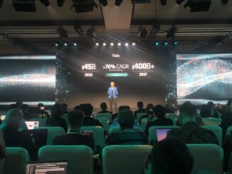
The Tidal Wave Of Rising GPU TAM Raises All Boats
The world has gone nuts for generative AI, and it is going to get a whole lot crazier. Like $400 billion a year in GPU hardware spending by 2027 crazier. If you don’t think this is an enormous amount of spending, consider that the US Department of Defense, which is …
AMD’s Top Brass Take Another Swing At Intel With Milan Epycs
It has been a long time – more than 15 years – since AMD has been in a position to pressure larger rival Intel in supplying processors to server OEMs and ODMs for the datacenter. In 2003, the company was able to surprise an Intel that was looking to force …
Industry Behemoths Back Intel’s Universal Chiplet Interconnect
When the hyperscalers, the major datacenter compute engine suppliers, and the three remaining foundries with advanced node manufacturing capabilities launch a standard together on Day One, this is an unusual, significant, and pleasant surprise. And this is precisely what has happened with Universal Chiplet Interconnect Express. The PCI-Express interconnect standard …
Comments are closed.
And then there were 3 teams with AMD/Cray and IBM/OpenPower/Nvidia and Intel/partners. Looks like U-Sam is spreading it around in the name of supply chain wisdom, and that’s a very good thing to do with those Exascale Initiative funds. I do hope that some ARM, or even RISC-V, based systems get some US funding because the more the merrier with the less being too damn monopolistic and not really good for innovation or pricing.
The real question here is who will have the most vertically owned Exascale System IP and very proprietary IP(Intel, Nvidia) at that and who will have the more Open IP as that relates to the software/API stack, and even the Firmware stack.
AMD has its very open API(ROCm) stack while IBM/OpenPower has options for a full open source CPU BIOS stack as can be used on Power8/Power9. Intel is surely going to be trying its level best to keep as much as possible in-house and proprietary while Nvidia takes the vary same approach. AMD’s a breath of fresh air for the x86 ecosystem in an Epyc sort of manner that will help to lower costs and prevent vendor lockin with ROCm being no cost licensing based while CUDA has some up fron licensing costs in addtion to whatever programming/development costs that any project will have to incur.
Now if the DOE has just pushed more Money at getting more than just Samsung and SK Hynix into the HBM/HBM2 market place that would have saved billions of dollars and billions of kilowatt hours. But as it currently stands Samsung has damn near killed the consumer HBM2 market and forced Nvidia to avoid HBM2 on consumer GPUs and AMD to retrench into using more GDDR5X/GDDR6 in the consumer GPU market where that GDDR5X/GDDR6 is an energy hog relative to HBM2 but GDDR5X/GDDR6 costs much less currently because there are more suppliers in the market place for non HBM/HBM2 memory. Just think of all that Power Plant infrastructure costs and power that could have been saved if the DOE/EPA had made more funding available to get more players started up in the HBM/HBM2 market place and all that coin mining was done mostly on consumer GPUs that used mostly GDDR5/GDDR5X and GDDR6 at the costs of billions of extra kilowatt hours.
Shame on you DOE and EPA and the US Government needs to maybe add some OEM Tax incentives to foster more HBM2 adoption among the various OEMs/ODMs and more low interest loans to some US memory maker/s to get more HBM2/Newer-HBM production and competition up and running among more than just 2 HBM/HBM2 suppliers.
https://www.anl.gov/article/us-department-of-energy-and-intel-to-deliver-first-exascale-supercomputer
The A21 system at Argonne will also use slingshot, not omni-path.
Also, don’t write off HPE as a possibility for El Capitan.
Yup. Just an old piece of data caught in my L2 cache.
I have been reading NextPlatform for years but never commented, so hi! Love the content here/
Ever since the announcement this morning for Frontier and AMD being pinned as the main supplier of the chips in question (GPUs and CPUs), I have been speculating on the speeds and feeds on this. Lisa mentions that the CPU part is a “beyond Zen 2” with AI and HPC custom bits built in as well as the same with the GPU part, I wanted to speculate on how fast these parts would from the chip level up to the 1.5 EFlops level.
A lot of it is just some stuff I threw together in Excel and based off some readings on the 64-port count on the Slingshot switch (https://www.cray.com/blog/meet-slingshot-an-innovative-interconnect-for-the-next-generation-of-supercomputers/), my own speculation on what a custom blade would be like (probably similar to the one from SC18 all water cooled in a single U) at 2 CPUs per blade and 8 GPUs per blade (but at node level, 1 CPU and 4 GPUs), and that there would be a total of 64 blades in a single cabinet to hook up to the Slingshot 64-port switch.
If Frontier were to get to 1.5 EFlops, I guessed at a custom Radeon Instinct GPU to be based on a GPU chiplet package. This package would house x8 (2048 shaders or cores each) chiplets surrounding a beefy I/O die (HBM and IF controllers) to make a cross shape with the chiplets. The chiplets would connect the the I/O die with IF links. Then HBM3 at 2 TB/s (or maybe 4 TB/s) and maybe 64 GB (or 128 GB) total VRAM and would be tied to the I/O die as well. With a total of 16,384 cores in the package, a 1.8 GHz clock (maybe 7nm+ on TSMC or something smaller maybe), kicking out about 59 TFLops SP or about 29.5 TFlops for DP. The entire package would probably be socketed for repair/maintenance and have a cold plate on-top with the water cooling. I am assuming x8 GPUs per blade (x4 per node), 64 blades per cabinet, and 100 cabinets total. For GPU power alone, I am guessing around just above the 1.5 EFlops. The GPUs would also be linked to their respective CPUs over IF.
To get clear above the 1.5 EFlops, the custom Epyc chip would need to achieve around 2.4 TFlops. This fits for what we know about Rome as it will provide x4 floating point performance above their fast Epyc, the 7601 around 600 GFlops (http://www.crc.nd.edu/~rich/CRC_EPYC_Cluster_Build_Feb_2018/Installing%20and%20running%20HPL%20on%20AMD%20EPYC%20v2.pdf). x4 of that would be 2400 (2.4 TFLops) and be still at 64 cores and around 2.7 or 2.8 GHz. Unless AMD has increased the core count for this custom Epyc (like 72, 80, or 96 cores and lowered the clocks to achieve the same TFlops count for the CPU). CPUs would probably be socketed for repair/maintenance and would also have the cold plates with the water cooling. Assuming x2 CPUs per blade (x1 per node), linked with their respective x4 GPUs using IF, 64 Epyc CPUs per cabinet at 100 cabinets, around 30.7 PFlops total from the CPUs alone. Combine the GPU count together, total around 1.54 EFlops.
Design of the nodes and blades would I imagine would be hot-swappable. You can take out the entire blade or just one of the nodes in the blade. And some sort of quick disconnect system for the interconnects, power, and the water cooling. Also having each blade have a dedicated 200 Gb/s port to the Slingshot switch
Memory my guess would DDR5 at 4TB per socket using the same channel count at 8 and each DIMM to be also water cooled.
Storage I wouldn’t have a clue, maybe have a bunch of NVMe arrays at the bottom connected to another switch at the top dedicated to the cabinet or have them alternating between the blades so each blade has a dedicated 1U NVMe (ruler style) array connected. Perhaps using Gen-Z for the storage interconnect between the computer blades and the NVMe arrarys and PCIe 4 or PCIe 5 for between the storage controllers and the rulers.
Anyway, sorry for the long comment. Keep up the good work and for keeping another long time reader!
Not by 2021 for any Multi-Die GPU on an MCM(PCB or Interposer) based package. And I’m sure that Crey/AMD is working up some Epyc/Rome Based variant in which to test out that xGMI(Infinity Fabric) based CPU to GPU coherent interfacing. Look at the first generation Zen Epyc/Naples and that supported that Infinity Fabric Based xGMI IP but that was only used for the IFIS(Infinity Fabric InterSocket) for CPU to CPU coherent interfacing across the SP3 sockets on the 2P Epyc/Naples MB platform. So 64 PCIe lanes from each Epyc/Naples MCM/Socket had their PCIe/PHY switched out from using PCIe protocol to using that xGMI/Infinity fabric based Protocol for the intersocket communication between the 2 processors on the Zen/Naples platform, and that will remain similar for Epyc/Rome also. Epyc/Rome is using Infinity Fabric Ver 2 at 2.3 times the per pin transfer rate compared to IF Ver 1.
The Vega 20 GPU base die tapeout does offer xGMI/Infinity Fabric support for up to 4 Radeon Instinct MI50s/MI60s to speak infinity fabric across a dedicated 4 GPU bridge connector that slots in across the top of up to 4 Radeon Instinct MI50/MI60 Discrete GPU accelerator cards.
AMD’s Navi is not going to be based on any multi-GPU die/chiplet designs as was implied by AMD/RTG new director as there are still technical issues to be worked out and designs have to be frozen at least a year in advance to allow for sufficient time for proper vetting and certification of hardware and the Software ecosystem that this exascale system will be using. But AMD did say that there will only be a Monolithic GPU die for any Consumer/Navi products so it’s still possible that Professional Navi in 2020 may have the beginnings of some form of scalable Navi/Newer GPU Die/Chiplet on an MCM package but that’s really not known currently.
Now the question that can be asked for Epyc/Rome and its Motherboard platform is will Epyc/Rome also support that GPU direct attached accelerator xGMI/IF based IP for direct/coherent CPU to GPU interfacing that is similar to what Nvidia offers for OpenPower power9 where Nvidia’s GPUs interface with OpenPower Power9 CPU via NVLink-2.
AMD’s representatives in advance of AMD’s first generation Zen/Naples product release did mention in a YouTube video that GPU direct attached xGMI/IF interfacing was possible for that platform and that was at an Oil industry related trade show/event where some initial benchmarking of Zen/Naples engineering samples where being shown.
So it appears that xGMI/Infinity fabric has been baked into AMD’s Zen CPUs and even Vega/newer GPUs but the full implementation had to wait for Vega 20 and possibly Epyc/Rome’s release hopefully for some Zen-2 CPU to Radeon GPU direct xGMI/IF interfacing to appear. Really AMD needs to match Nvidia’s NVLink/Power9 interfacing feature for feature for the regular server market on Epyc/Rome so Epyc/Rome should have that xGMI/IF CPU to GPU interfacing offered to be competitive with Power9/NVLink-2 and Nvidia GPU accelerator offerings.
AMD’s Radeon Pro V340 utilizes AMD’s MxGPU ASIC Die IP that’s used to interface 2 Vega 10 GPU dies on that single PCIe card based V340 server variant and that MxGPU IP manages in its ASIC Hardware/Firmware all the necessary SR-IOV support to allow the dual Vega 10 dies to be virtualized up into many logical GPUs and passed through to containerized or VM based OS instances. So AMD has already the ability to create Dual GPU Die based SKUs for several generations before Vega was introduced and that Radeon Pro V340 SKUs that’s based on dual Vega 10/14nm GPU DIEs will be updated to Vega 20/7nm and maybe that MxGMU ASIC Die will pick up some xGMI Infinity Fabric support in addition to SR-IOV support in its hardware. So maybe some Dual Navi 20 GPU dies on a single PCIe card will be utilized in the Crey/AMD Frontier Exascale system.
I’d expect that that Crey/AMD will have an upgrade contact in place with the DOE for some lifetime upgrades of that platform to newer IP and better power/performance metrics over time before the system’s usable lifetime expires and that system is completely replaced.
The NextPlatform did have an article with a PDF referenced for and AMD “Exascale APU” based system in a Research Paper commissioned via and earlier round of US government Exascale Initiative funding. But I do not think AMD is far enough along with that IP for it to be fully implemented in time for the Frontier Exascale system’s release. Things appear to be progressing more at an evolutionary pace than a revolutionary pace as is the norm for these types of contracts.
Good heavens. More commenters like RTone, please! Nice work.
I don’t envy Cray at this point. Three upcoming DOE Shasta/Slingshot systems: 2020, NERSC-9 Perlmutter, with future AMD CPUs and future NVIDIA GPUs. 2021, Coral 1.5 Aurora at Argonne, with future Intel CPUs and future Intel X3 GPUs. 2022, Frontier, with future+ AMD CPUs and future+ AMD GPUs. Very similar physical structures, but with very different programming strategies. This will stress the programming environment team, unless Intel and AMD are going to take control of that for the latter two systems, in which case the programmer community takes it on the chin (HIP vs OneAPI).
Michael Wolfe: What do you mean by different programming strategies? It would seem that all of these designs are pretty similar, despite using components from different manufacturers. 1 CPU socket + several GPU sockets all tied to several high speed NICs. Even intel gave up on using vectorized atom cores ala xeon phi, and has a more or less standard GPU architecture. From a programming standpoint you have a couple dozen fast scalar cores controlling ~4 collections of a couple thousand-ish vector cores. There’s some back-end differences in how you lay out vector streams in the hardware, and the size and number of memory interfaces, but the compiler front-end and general programming environment should be remarkably similar from one parallel-GPU system to the next. I’m not an expert in the area, but I suspect helping the programmer to code to the architecture is the bigger challenge for the compiler, than actually placing that code on the GPU.
What I’m interested in is how many mpi ranks each node will run. Can they stripe across all GPU such that each node can run a single rank? Obviously you can do that with layered MPI on top of openMP, but can they do that with only one scalar rank? Would it run well?