

There is a rumor going around that a certain hyperscaler is going to be augmenting its GPU-based machine learning training and will be adopting Intel’s Nervana Neural Network Processor (NNP) for at least some of its workloads. Some of the chattering lends itself to hyperbole, claiming that Facebook, the operator of the world’s largest social network, would do all of its machine learning training on the Nervana NNPs once they are widely deployed and, by implication, would be using Intel accelerators to do inference as well.
We are not so sure we believe that, and it would be very hard to verify that. What we know for sure is that Facebook has rearchitected its machine learning infrastructure for both training and inference so it could easily slip different kinds of compute into its infrastructure, as we discussed while attending the Open Compute Project’s Global Summit 2019 last week. One of the innovations that Facebook has created in conjunction with Microsoft and in support of other hyperscalers such as Google, Alibaba, Baidu, and Tencent, is the OCP Acceleration Module, which is a common accelerator form factor that is basically a portable socket (handle included) that plugs into a PCI-Express switch fabric. Chip makers AMD, Graphcore, Habana, Intel, Nvidia, and Xilinx have all agreed to adopt this OAM form factor, and it would not be surprising to see Google do the same thing with its TPU 3.0 machine learning accelerators.
It may be a coincidence, or it may not be, that Intel was on hand at the OCP conference to talk about how to deploy the “Spring Crest” Nervana NNP-L1000, a follow-on to the “Lake Crest” NNPs that we detailed a year ago and that Intel has now characterized as a development platform. Last summer, Naveen Rao, general manager of the AI group at Intel, said that the Spring Crest NNP would have somewhere between 3X and 4X the training performance of the Lake Crest NNP, and didn’t say much more about its architecture beyond that. Song Kok Hang, senior manager of system design at the chip maker, showed off an OAM module implementation of the NNP-L1000, the back and front of which are shown below:
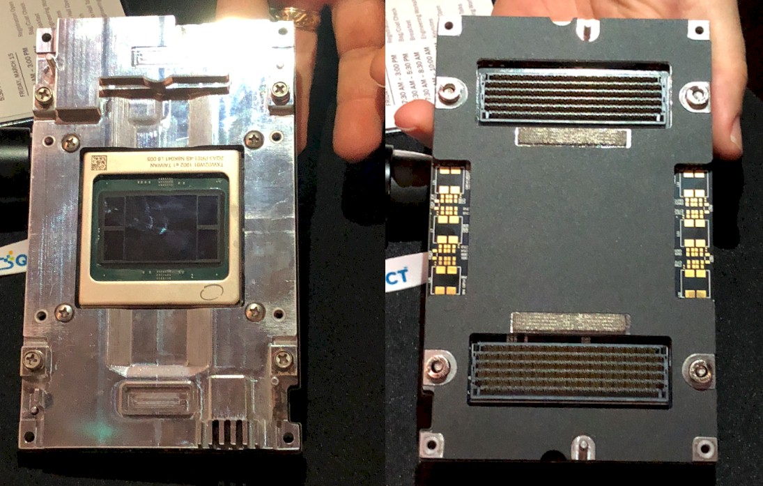
Hang also talked a bit about the OAM mezzanine module specification for the future Nervana NNP, which provides some insight into that accelerator. Like other OAM modules, the mezzanine card measures 102 millimeters by 165 millimeters, and in this case there are two variants, one rated for NNPs that consume 200 watts and another that consumes 425 watts.
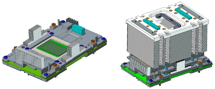
Here are the mechanicals that show the populated NNP-L1000 mezzanine module for the OAM, without and with the handled heat sink added to it:
The OAM can take in voltage at 3.3 volts or in a range from 40 volts to 60 volts, depending on the rack power. The OAM setup in the “Emerald Pools” accelerator enclosure of the Facebook “Zion” server can handle up to eight of the NNP-L1000 processors rated at 425 watts for a total maximum power of 3,400 watts, still with passive air cooling with input air as high as 35 degrees Celsius (95 degrees Fahrenheit).
The NNP-L1000 processor has a total of 16 inter-chip link (ICL) SerDes circuits, which are carved up into 16 ports with four lanes of traffic each. Here is the block diagram of what it looks like:
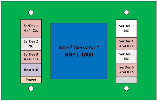
Those four ICL SerDes are show in pink in the block diagram. There are three other SerDes that are not used, which presumably could be used to drive more interconnect ports out of the chip for even tighter meshing of the NNPs or a larger network of them. There are also separate circuits for the PCI-Express x16 link to the host, presumably a 4.0 generation link timed to the launch of the “Ice Lake” Xeon SP processors coming later this year but also possibly also supported lower speed PCI-Express 3.0 links that run half as fast.
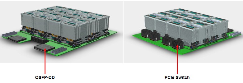
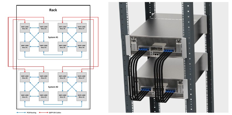
The NNP-L1000 accelerators are linked to each other in a hybrid cube mesh topology, which is what is commonly used to cross-couple GPUs to each other in hyperscale systems with eight Tesla accelerators in them. The Intel OAM design for the Nervana chips uses a combination of routing done on the Emerald Pools circuit board and external QSFP-DD cabling, which was created to support 200 Gb/sec and 400 Gb/sec Ethernet. This mechanical shows where the four PCI-Express switches and the two quad-port Ethernet NICs that make this hybrid cube mesh are located:
In the block diagram, the PCB interconnects are shown in blue and the QSFP-DD links are shown in red, but in the picture, the QSFP-DD cables have blue pull tabs. So keep that in mind when you are interpreting things by color. Here is what a single chassis using the Nervana OAMs looks like:

And here is how two enclosures, with a total of sixteen Nervana NNP-L1000s would be linked together:
This is not the end of the scalability. You could put two of these enclosures in a pair of racks, for a total of four OAM trays, and link them up this way:
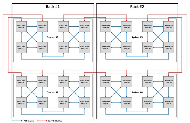
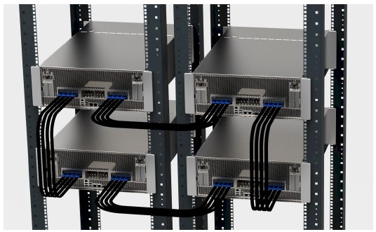
And the physical machines would be cabled like this:
Given that this is all using standard PCI-Express on the system board and QSFP-DD ports, there is nothing about this topology that can’t be applied to other accelerators. And that is the beautiful thing about the open source hardware specifications of the Open Compute Project. Someone could do the same thing with Nvidia Tesla GPU accelerators and create a poor man’s DGX-2 that has 32 GPUs cross linked – admittedly with a lot less bandwidth linking the GPUs (well, one sixth than of the NVSwitch if you used PCI-Express 3.0 x16 ports on the Emerald Pools board) and without memory atomics across those GPUs. But for some neural networks and their frameworks, that may not be as big of a deal as we think.
It will be interesting to see these ideas play out in production, that we know for sure.

Oracle Still Hanging In There With Exadata Engineered Systems
It may not seem like it, but Oracle is still in the high-end server business, at least when it comes to big machines running its eponymous relational database. In fact, the company has launched a new generation of Exadata database servers, and the architecture of these machines shows what is …

Covering All The Compute Bases In A Heterogeneous Datacenter
Intel has spent more than three decades evolving from the dominant provider of CPUs for personal computers to the dominant supplier of processors for servers in the datacenter. While Intel has argued that Moore’s Law is not dead – that the pace of innovation with transistors and therefore semiconductors has …
AMD Now Has More Compute On The Top500 Than Nvidia
There has been a lot more churn on the November Top500 supercomputer rankings that is the talk of the SC24 conference in Atlanta this week than there was in the list that came out in June at the ISC24 conference in Hamburg, Germany back in May, and there are some …
The infrastructure around that processor reminds me of Itanium. Did Itanium also dissipate power at the rate of 400 odd Watts?