

Constructing a processor from an entire silicon wafer might seem like a strange idea, but a new study demonstrated that a waferscale chip can outperform an equivalent multi-chip module MCM by an order of magnitude, while delivering much better energy efficiency.
The concept of waferscale integration (WSI) is fairly simple: instead of manufacturing a wafer full of chips, only to slice them apart and then wire them back together on a printed circuit board (PCB) in multi-chip module or package, the wafer itself can serve as the substrate for a “super-chip,” with individual components wired together in place. Theoretically, this should cut costs (packaging up the individual dies is eliminated) and improve performance (faster data rates can be achieved through proximity of the components).
WSI also enables much denser devices to be constructed. In a package, 90 percent or more of the real estate is devoted to non-die componentry. And according to Intel, the I/O circuitry for chip-to-chip communication already accounts for more than 25 percent of the area on some processors. With a waferscale device, less than 10 percent of area would be taken up by interconnects.
The idea to build waferscale chips has been around for a while. One of the most notable attempts was in 1980, when Gene Amdahl tried to construct a mainframe waferscale computer chip as the basis for his newly founded startup, Trilogy Systems. Like other attempts at WSI during the 1970s and 1980s, Amdahl’s effort failed principally because semiconductor manufacturing yields at the time weren’t good enough to produce the requisite number of usable wafers.
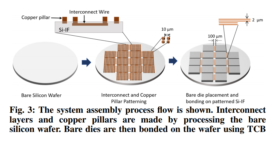
Since then, manufacturing has advanced significantly, and new techniques have emerged that offer some intriguing possibilities for WSI. In particular, the researchers point out that it’s now possible to bond high-yielding dies of processors, memory modules (including 3D DRAM stacks), and even peripherals onto a wafer and connect them using a new wafer-level interconnect technology, known as Silicon Interconnect Fabric, or Si-IF.
The study in question today was conducted by a team of researchers from the University of California, Los Angeles (UCLA) and University of Illinois at Urbana-Champaign (UICU), was described in a paper titled Architecting Waferscale Processors – A GPU Case Study.
The UCLA-developed Si-IF technology offers considerably better bandwidth, latency, and energy efficiency than package-level interconnects, although not quite as good as on-chip links. The Si-IF base material is integrated with copper pillar I/O pins and inter-die links, which serve as the high performance data pipes for the wafer. In essence, Si-IF replaces the PCB with a silicon substrate and allows dies to be bonded directly to the wafer.
There are commercial multi-die interconnects available today, namely TSMC’s Chip on Wafer on Substrate (CoWoS) and Intel’s Embedded Multi-die Interconnect Bridge (EMIB), but according to the researchers, these technologies have limited scalability. The largest CoWoS device today comes with a single GPU and four memory stacks, while the EMIB technology can only hook up about 5 to 10 dies.
To demonstrate the readiness of technology, the researchers constructed a 100mm prototype wafer with ten 4mm2 dies bonded to the Si-IF substrate and connected with 40,000 copper I/O pins. In testing the electrical connectivity across the dies they determined that all of the pillar pins and the inter-die links worked as expected. “The high yield we observed for this prototype, coupled with high yield reported previously for bonding of dies on Si-IF, demonstrates the technological readiness for building waferscale systems,” write the researchers. Keep in mind that the dies here are “pre-manufactured” separately. They are not being etched directly on the wafer.
The rest of the study involved comparisons of “hypothetical” waferscale GPUs against various configurations of single-chip and multi-chip GPUs (in this case, four GPU modules per package). The researchers selected GPUs as the basis for their case study because the applications that run on them tend to be highly parallel in nature, so are a good architecture to demonstrate the advantages of multi-die integration. To measure application performance, the researchers chose seven different benchmarks that spanned physics simulations, machine learning, linear algebra, medical imaging, graph coloring, and social media.
A 40-GPU wafer ran these benchmarks an average of 5.2x faster, and a maximum of 18.9x, compared to a scaled-out 40-MCM configuration (a board of ten four-GPU packages). The 24-GPU wafer outran its competition (a board of six four-GPU packages) by an average of 2.3x, and a maximum of 10.9x. The researchers attributed the speed-ups to the Si-IF’s higher data bandwidth compared to the on-board network in the MCM configurations.
Likewise, based on the energy-delay power (EDP) metric, the hypothetical GPU wafers demonstrated much better energy profiles running the benchmarks compared to their MCM counterparts. According to the simulations, the 24-GPU and 40-GPU wafers were 9.3x and 22.5x more energy efficient, respectively. The researchers credited the better results on the waferscale hardware to the significant reduction in execution time, as well as the superior energy efficiency of the wafer-level communication.
The wafer GPUs they devised ran at a relatively modest clock speeds: 575 MHz for the 24-GPU one and 408 MHz for the 40-GPU version. If higher frequencies could be used, the researchers claim their performance advantage would also increase, albeit modestly: a 1 GHz 24-GPU wafer would outperform the scaled-out 24-MCM by an additional 7 percent.
One key advantage of WSI that was only touched on in the paper was the fact that each multi-GPU wafer would appears as a single super-sized GPU to software. Even if the performance and energy advantages were only modest, the increase in programmer productivity alone might make this technology extremely attractive to developers.
Whether WSI ever makes it out of university labs remains to be seen. Commercial viability is often a tricky thing, even with technology that appears to be poised for productization. If these researchers really believe waferscale is ready for prime time, perhaps a spin-off is in the cards.


Mainstream Waferscale Closer Than It May Appear
The term “mainstream” in the context of the largest systems on the planet still only means a select few. But it is quite possible that proofs of concept for the sites building those huge future machines could set the stage for what’s next in some of the most demanding compute …
TSMC Makes The Best Of A Tough Chip Situation
If you had to sum up the second half of 2022 and the first half of 2023 from the perspective of the semiconductor industry, it would be that we made too many CPUs for PCs, smartphones, and servers and we didn’t make enough GPUs for the datacenter. Or rather, Taiwan …

Cerebras Needs Wall Street To Expand Beyond One Core Customer
Waferscale compute engine and AI system maker Cerebras Systems has filed with the US Securities and Exchange Commission to sell a chunk of itself to the public, giving we outsiders a view of the past two and a half years of its internal financials. Those financials reveal how much Cerebras …
These ideas could be used also to develop an sql/database processing unit aka SQLPU.
Another possible application for such waferscale integration is simulating a switch chip with a very large number of ports by building an entire CLOS network on a wafer.
I would imagine that using WSI will have negative effect on yields.
Assume we’re building an chip that’s composed of 4 chiplets connected by Si-IF.
If one of the chiplets fail, or the Si-IF bind itself fails, you lose all four chips.
More-ever, the number of active cores, speed, will be limited by the slowest chiplet.
Whereas normal MCM, you can simply cherry pick the best chiplets and create a high end CPU/GPU (E.g. 64 core, top of the line chip); and use the partially damaged chiplets and use them for low-end CPU/GPU (E.g. 32 core, mid-end CPU).
Totally agree with Gilboa Davara. Adding that the process node would make the biggest hinderance – at any processing node each chip etched on that wafer is the same price, smaller is profitable, with this method the wafer is sliced relative to GPU equaling bigger portions of the wafer. I know these are hypotheticals but it just doesnt meet the smell test vs profitability for a 7% increase vs MCM??
Ignore the 7% comment – these cards are obviously highest end enterprise @ 5-18X speed gains.