

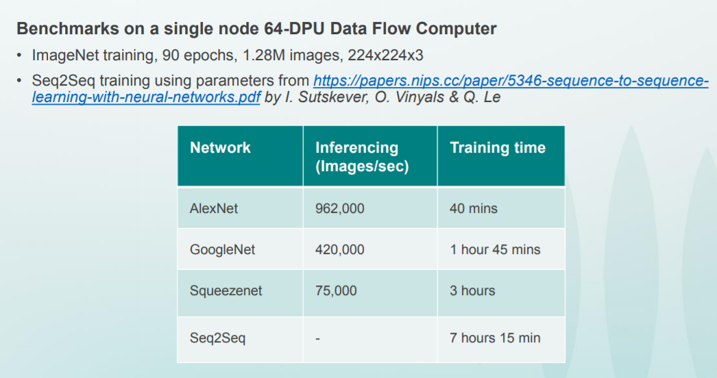
Propping up a successful silicon startup is no simple feat, but venture-backed Wave Computing has managed to hold its own in the small but critical AI training chip market–so far.
Seven years after its founding and the company’s early access program for beta machines based on its novel DPU manycore architecture is now open, which is prompting Wave to be more forthcoming about the system and chip architecture for deep learning-focused dataflow architecture.
Dr. Chris Nicol, Wave Computing CTO and lead architect of the Dataflow Processing Unit (DPU) admitted to the crowd at Hot Chips this week that maintaining funding can be a challenge for chip startups but thinks that their architecture, which they claim can accelerate neural net training by 1000X over GPU accelerators (a very big claim against the dominant architecture for deep learning training), will take off after some early customers and benchmarks prove their points.
Their view is that dataflow architectures are the only way to efficiently train networks with high performance. The CPU is carved out of their systems entirely and as we explained when first details were clear about what they were working on in depth last year, the Hybrid Memory Cube does a great deal of the heavy lifting in terms of both compute and data flow. We now have far more detail than we’ve seen to date about how it works—and where it might carve out market share in the future.
Nicol is no stranger to applying manycore strategies to targeted problems. He helped established Australian R&D organization NICTA, which focuses on embedded manycore systems and software and founded Bell Labs Research in Australia where he co-developed one of the first multiprocessor SoCs. While deep learning training is not an embedded computing problem, Nicol says there is a day coming when even large-scale training will move out of the datacenter. Wave has not developed systems that fit this bill yet, but his background and this statement indicate there might be a research direction at the company to push more neural network training to the edge (as others are thinking). This is a place where its DPU elements could potentially have value in the future.
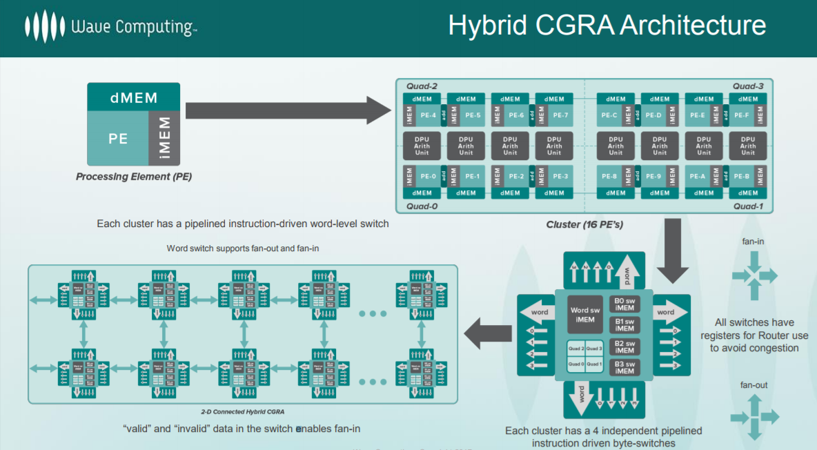
In the here and now, the chip has some very noteworthy features, and it actually gets more elegant from a larger scale-up system view. The DPU has 16,000 processing elements, over 8,000 arithmetic units, and a unique self-timing mechanism. Everything (all cores) run at 6.7GHz using a coarse grained reconfigurable architecture—a very different animal than what we have seen from some other deep learning chip startups. When no data is being fed through, the DPUs go to sleep. The DPU can be considered as a hybrid FPGA and manycore processor that tackles static scheduling of data flow graphs across these thousands of elements. Take a look below.
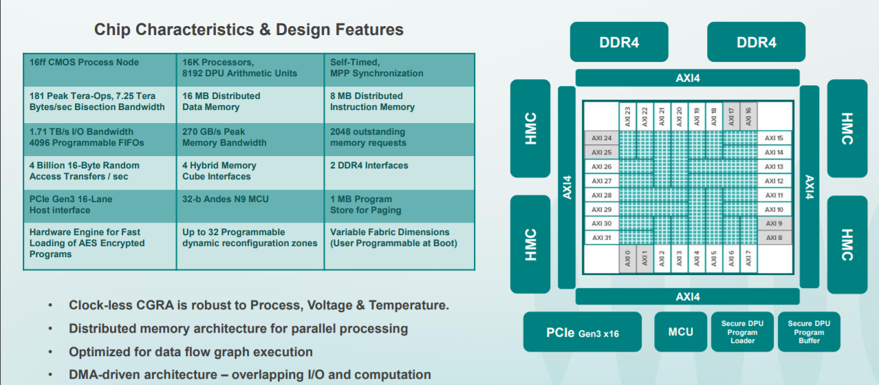
The graphic above shows four DPUs on a board with a cascading use of the HMC devices. The DPUs actually have quite a bit of interconnectivity through the HMCs, so if a dataflow graph is being executed, most of the communication is local from node to node in the graph. Wave lightly described a “balancing mechanism” to balance the delays through the execution of the graph via buffers between the nodes. By injecting some latency throughput is balanced through the graph and utilization increases. The tensor data for something like TensorFlow (native in the early access machines) is stored entirely in HMC, which means there is not much networking needed between the DPUs. In short, most of the data rides through the HMCs.
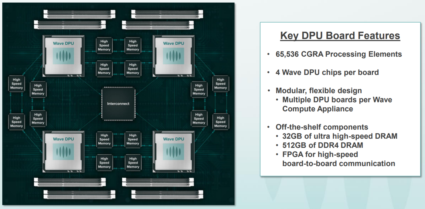
The following image shows 16 of these boards in a cluster, connected to a large block of memory with each having its own personal instruction memory. These are 8-bit which means they can be run ala MIMD or ganged together to do SIMD operations at runtime. It is a data-driven machine as well, as mentioned, so when elements aren’t being used, the clocks are gated.

“The problem with the definition of heterogeneous computing today is it says the master or control always runs on the CPU and the accelerator is just dumb. This means your runtime API runs on CPUs and the slave has to wait for the CPU to tell it what to do. We want to get away from that,” Nicols says.
He points to how accelerator architectures (GPUs in particular) suffer from the lag when new kernels are being loaded and how they get around this by using an MCU for moving programs in and out at runtime. The programs themselves determine when this happens (there’s no runtime API sitting on a host somewhere directing things).The programs communicate with this MCU, which DMA transfers the programs in and out of the chip and controls their propagate signals. There is also a program cache on the chip. The net result is a CPU-less architecture that Nicols says gets extra gains on these small but important hitches within an offload model.
No bias—it is the techniques like these that stack up to a very compelling architecture. Many modifications to both get around a lack of a CPU and new flexibility because of that missing overhead make this something worth watching in terms of performance and efficiency benchmarks this year. What kind of risk will be tolerated for the bigger hyperscalers that might consider a different mode of training is its own question since the software ecosystem for GPUs is by far the most robust for this growing class of workloads.
The nice thing about analyzing a hardware device is that it is pretty cut-and-dry. Facts are facts. But where things get fuzzy, especially for new architectures is how the software operates (and how users interact with it). “Deep learning is really a dataflow graph programmed on top of deep learning software and run on a processor like ours that can assemble a dataflow graph at runtime,” Nicols says. “The workflow generates the dataflow graph to train the network; at runtime we take that dataflow graph from TensorFlow, for example, and convert that at runtime directly into a dataflow graph that executes without the CPU and maps onto our dataflow chips.”
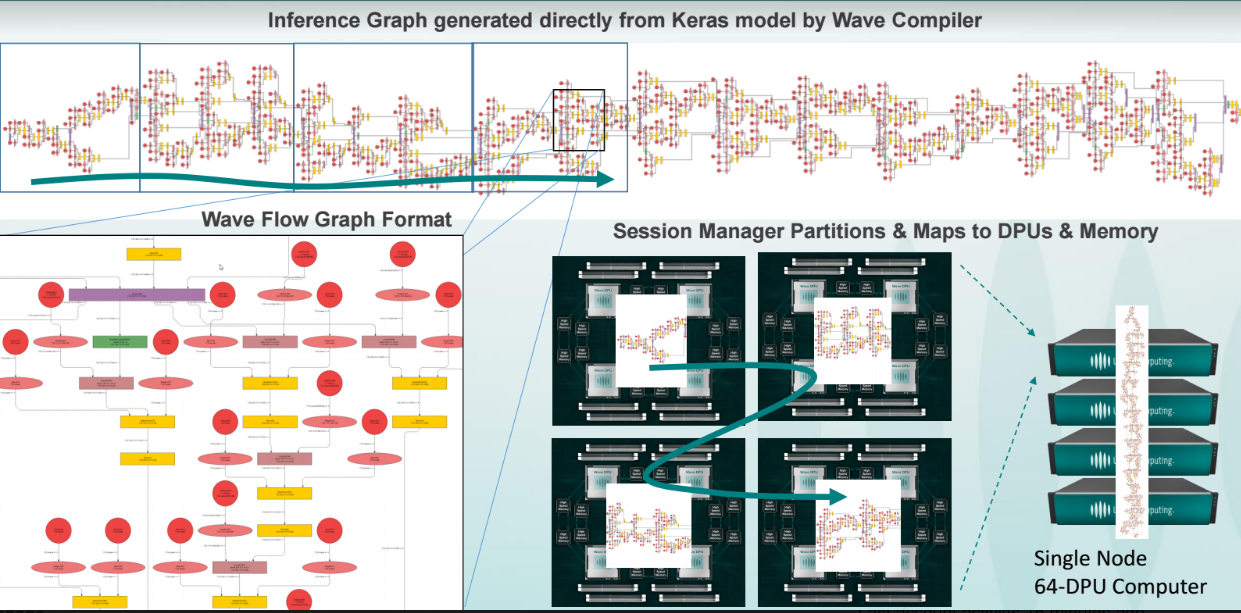
“This is a coarse grained, reconfigurable array—it is akin to spatial computing. When a program compiles to a many-processor core, it is still necessary to partition that program into threads that run across those. That is the problem with having so many cores on a chip—programming. OpenCL is not an answer here,” Nicol says. Although he did not name the high-level language, it is used it used to partition the training set into a dataflow graph with Wave’s own spatial complier tools to schedule, route, and map software onto their tightly coupled interconnected fabric of processors. Here, it is faster to let processor neighbors talk to each other (versus using registers).
We will follow this hardware story with a software-focused one that covers the stack, much as we did with deep learning chip startup (and Wave rival) Graphcore (hardware story here and software piece here).
If you’re really interested in Wave, looking up their publicly available patent info is worth the time. This will help explain in far more detail some of the self-timing mechanisms, HMC interfaces, and compiler strategies in particular.


WOW that looks mighty impressive a very different approach. The problem is probably the dataflow graph and how flexible it can be.
Especially if we’re moving to multiple networks soon and they need to interact / share weights, data.
not flexible enough, you can be very fast but you need to move the data back and forth… that is the bottleneck now!
Alexnet can be done in 18 min on a Nvidia DGX-2 (according to Nvidia)
Already on the market.
I wonder when would these be on the market in order to compare price, power consumption.