

With Intel having significant difficulties in ramping up its 10 nanometer manufacturing processes and not really talking much about its plans for 7 nanometers, there has never been a better time for its few remaining rivals in chip manufacturing to give their respective CPU and GPU customers and edge to carve out some market share in the datacenter and on the desktop, which helps cover the cost of being in the datacenter because it helps ramp advanced processes.
AMD can deliver as many cores and as much memory bandwidth as Cavium can with its Arm ThunderX2 chip, and it can beat IBM’s Power9 in memory bandwidth and deliver 33 percent more cores to boot. We don’t know if Qualcomm’s Centriq 2400 is still a contender, with the company not being clear if it intends to stay in the server racket. But what we can say for sure is that AMD has one advantage that no Arm or Power chip has: It runs the X86 instruction set, which means it can run a great deal of code in the enterprise and among HPC, hyperscale, and cloud builders unmodified. To be sure, code needs to be tweaked and tuned to run best on any architecture, and over time this will happen with AMD’s Epyc 7000 series of server processors.
But having a performance and price/performance advantage at 14 nanometers is not going to be enough for AMD to capture the kind of client and server market share that it wants to with its respective Ryzen and Epyc chips, and it is also not sufficient for AMD to start taking some GPU share – particularly when it comes to GPU compute, not device graphics – away from Nvidia. So, after hedging its bets and backing 7 nanometer processes from both Taiwan Semiconductor Manufacturing Corp and GlobalFoundries for its CPUs and GPUs, AMD is putting the pedal to the metal – well, the accelerator to the silicon etcher – and moving up the use of 7 nanometer techniques for its “Vega” GPUs and keeping to its word to sample by the end of this year the “Rome” Epyc processor, the kicker to the current “Naples” Epyc 7000 that was launched in June last year.
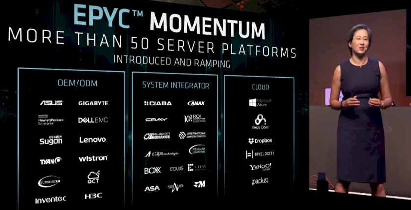
The speedup in the GPU roadmap and the reaffirmation of the CPU roadmap come as the Epyc processors have chalked up more than 50 design wins among OEMs, ODMs, and cloud builders, importantly including new servers from Hewlett Packard Enterprise and Gigabyte and a cloud instance from Chinese hyperscaler and public cloud provider Tencent and hot on the heels of the new modular machines from Cisco Systems, which we covered last week. (We will be taking a deep dive on this new Epyc iron from HPE and Gigabyte as well as the Tencent cloud instances based on Epyc separately. Stay tuned.)
Pushing Performance, Then Pushing Process
During her presentation at Computex, Lisu Su, AMD president and chief executive officer, stressed the fact that AMD was about pushing the performance envelope once again, and that it has seen good traction across its Ryzen and Epyc CPUs and Radeon and Radeon Instinct GPUs because of this transformation. As an underdog, AMD has to push the architecture first, and then push the process – and that is what makes AMD different from Intel, which has always thought of itself as a manufacturer first and a designer second because, quite frankly, as the dominant supplier of processors for clients and servers it can afford to do it that way around.
“We are absolutely about high performance computing,” Su explained, and she was not just talking about traditional HPC simulation and modeling workloads that we talk about here at The Next Platform, but high performance in its many guises. “We are not just about building great products. We are about changing and redefining the industry.”
On the Ryzen front, these client chips based on the “Zen” core have had over 20 product design wins for mobile and desktop products, with the biggest and most important suppliers being Dell, HPE, and Lenovo and with over 5 million shipments to date. For Radeon, which includes regular GPUs for graphics as well as the Radeon Instinct GPU accelerator cards for HPC and AI workloads, Su dropped these tidbits: Shipments of the current “Vega” GPUs for PC and console devices, which launched in August 2017, are more than ten times that of their predecessors even though they are only nine months old. This is a very good ramp, and it means – we hope – that AMD will be generating enough cash from GPUs for some big architectural advances in the future “Navi” GPUs that will bring it closer to parity with Nvidia compute GPUs on double precision and other mixed precision integer and floating point. This is key for AMD to get more traction in the HPC and AI spaces, which is where a lot of the margin in servers is these days.
Here’s the interesting bit. As you can see from the roadmaps that were put out last June, the original plan was to do a refined 14+ nanometer kicker to Vega and then move to Navi at some point about halfway between 2017 and 2020. The new roadmap now shows a Vega kicker coming in at 7 nanometers this year, with the Navi at 7 nanometers following and then a “Next-Gen” and as-yet unnamed follow-on GPU using a 7+ nanometer process tweak coming around 2020. It is beginning to look like the 7 nanometer manufacturing is coming along a little better than expected and AMD can make a bet on just shrinking the Vega to boost the performance – and do it this year.
To be precise, the Vega shrink to 7 nanometers is actually sampling now, and will be shipping sometime in the second half of 2018, and Su did a bit of show and tell to prove that the chip existed:

By moving to the 7 nanometer processes, the transistors on a chip have twice the density of etchings done with 14 nanometer processes, and given the shrinkage in the circuits and the roughly doubling in the power efficiency, the clock speeds can be inched up. AMD expects to deliver about 35 percent more performance with the 7 nanometer processes as well as twice the power efficiency over circuits designed using the 14 nanometer processes at GlobalFoundries, which is making the current Vega GPUs and Epyc CPUs. Importantly, the coming Vega+ GPU has four ranks of HBM2 stacked memory, for a total of 32 GB of capacity, four times that of the Vega 10 chips used in the current Radeon Instinct GPU accelerator cards. This is parity with the HBM2 memory capacity on the latest “Volta” GV100 GPUs from Nvidia. Not surprisingly, this Vega+ GPU will be used first in the Radeon Instinct line, where AMD can charge a premium to HPC, AI, and cryptocurrency mining customers.
As for servers, the Rome Epyc chips are going to go straight to the Zen 2 core and 7 nanometer processes and skip the Zen+ tweaked core that will be coming out in Ryzen chips later this year in a ThreadRipper version for extreme performance, based on 12 nanometer process (probably the same one from TSMC that Nvidia is using to make the Volta GPUs). The desktop Ryzen chips based on 12 nanometers and Zen+ cores shipped in April.
The Rome Epyc chips will be socket compatible with the current Naples Epyc 7000s, and that suggests that the I/O lanes will stay the same at 128 per socket and that the memory bandwidth could stay the same at eight DDR4 memory controllers per socket.
Su also showed off this Rome Epyc chip, just to complete the set:

There is a good chance that AMD will increase the core count and the memory controller count with the Rome Epyc chips – that is what we would do – and keep the heat on Intel in these areas. Adding more I/O lanes almost certainly would mean changing the Epyc 7000 socket, and AMD cannot afford to do that. Server makers cannot recertify a whole new hardware platform with each generation. It is not at all clear if the “Milan” Epyc chips, due around 2020, will have a socket upgrade, but we know they will be based on a 7+ nanometer process and use the Zen 3 cores.
Your move, Intel.

The Next – And More Profitable – 10 Percent Of Server Share For AMD
When this is all said and done, Intel will deserve some kind of award for keeping its 14 nanometer processes moving along enough as it gets its 10 nanometer and 7 nanometer processes knocked together to still, somehow, manage to retain dominant market share in the server space. Or, maybe …
Nvidia Sacrifices Profits To Preserve Revenues In The US
Making a graphics card for gamers is one thing, but manufacturing a rackscale supercomputer with over 600,000 components that burns 120 kilowatts of power, that has over 5,000 copper cables for an all-to-all interconnect mesh for 72 dual-chip compute engines, and that weighs over 3,000 pounds is another thing entirely. …

Who Will Build Europe’s First Exascale Supercomputer – And With What, And Why?
Exascale supercomputing is just as important to Europe as it is to the United States and China, but each of these geopolitical regions on Earth has its own way of developing architectures, funding their development and production, and figuring out where the best HPC centers are to host such machines …
Well done Timothy. A very good treatment of this exciting historic contest.
I hope it is read widely.