

There is no question right now that if you have a big computing job in either high performance computing – the colloquial name for traditional massively parallel simulation and modeling applications – or in machine learning – the set of statistical analysis routines with feedback loops that can do identification and transformation tasks that used to be solely the realm of humans – then an Nvidia GPU accelerator is the engine of choice to run that work at the best efficiency.
It is usually difficult to make such clean proclamations in the IT industry, with so many different kinds of compute available. But Nvidia is in a unique position, and one that it has earned through more than a decade of intense engineering, where it really does not have effective competition in the compute areas where it plays.
Parallel routines written in C, C++, or Fortran were offloaded from CPUs to GPUs in the first place because the CPUs did not have sufficient memory bandwidth to handle these routines. It was convenient, perhaps, that the parallel engine used to produce graphics for games and virtualization could be tweaked so it could do raw compute for simulation and modeling. Intel’s “Knights” family of many-core X86 processors, with their own MCDRAM memory and extended DRAM architecture, were created explicitly to bring GPU-like performance to X86 computing, eventually without an offload model with the “Knights Landing” Xeon Phi 7000 processors. Nvidia has iterated fast with its Tesla family of GPU accelerators, and adding new functionality and extreme performance at a pace that Intel has not been able to match with the Knights family, and as good as AMD’s “Vega” GPU chips are, they only support half precision and single precision floating point math (which are suitable for machine learning, seismic processing, signal processing, bioinformatics, and certain workloads) and do not have the double precision floating point math that many HPC applications still require.
Neither has anything at all like Nvidia’s Tensor Core units.
In fact, no compute engine on the market has the breadth and depth of number crunching that the current “Volta” GV100 GPUs, which were launched last May, offer. There is no safer bet on which to make for running accelerated HPC applications or for going large scale machine learning training and, now, machine learning inference. The Volta processors are probably going to be the motors of choice for accelerated databases, too, but the jury is still out there. (FPGAs have their place here as well.)
From Graphics To General Purpose Compute
The GPU motor has come a long way since the “G80” GPU was launched by Nvidia back in 2006, laying the groundwork for what has evolved into the Volta GPU, arguably them most complex and rich computing engine yet put into the field for parallel processing. This GPU had eight shader cores, each with sixteen processing elements, introducing a much more parallel architecture than prior chips from Nvidia.
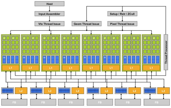
Although this is a very simple block diagram by today’s standards, the G80 chip was complex for the time. It was implemented in a 90 nanometer process with 686 million transistors and a die size of 480 square millimeters. Actually, this was a two-chip package, with the I/O broken out into a separate and small (about 5 million transistors) device.
The G80 was put into the GeForce 8800 graphics card, and came with this new thing called the Compute Unified Device Architecture programming environment, which allowed for parallel sections of math routines written in C to be offloaded to these special shader processing elements. Eventually a special variant of the GPU chip, called the GT200, was created for the first generation of Tesla T10 GPU accelerator cards and doubled the number of cores to 240 spread them over eight SMs, or 30 cores per SM, and added native double precision floating point math for supporting HPC applications.
But the ball really got rolling with the introduction of the “Fermi” GPU chips in 2010, which had 512 cores, supporting a mix of single precision and double precision floating point math over 32 streaming multiprocessors, or SMs.

Each Fermi GPU core, which was called a CUDA core back then, had a 32-bit integer unit and a 32-bit floating point unit, and importantly offered fused multiply-add operations, which is more efficient than prior multiply-add units that had two, rather than one, rounding step to perform their calculations. The important thing is that on matrix multiplication at double precision, the GF110 Fermi GPU, which weighed in at 3 billion transistors in a 520 square millimeter area die, could do one single precision FMA per clock or one double precision FMA every two clocks, which was 8X the floating point math of the GT200, which had only a meager double precision unit for each SM. With Fermi, the CUDA environment was expanded to support Fortran, Matlab, Python, and Java offloads.
We are going back to the beginning to show just how far GPU computing has come. (If you want to read the details on the “Kepler” GK104 and GK110 GPUs used in the K series of Tesla accelerators, here is a good place to start. You can see our coverage of the “Maxwell” GPUs used in Tesla accelerators from 2015 here, with our drilldown into the “Pascal” P100 GPUs for HPC and machine learning training here and the Pascal P4 and P40 units for machine learning inference there. The level of complexity in the Volta chips, which use a special 12 nanometer FinFET process that Taiwan Semiconductor Manufacturing Corp created specifically for Nvidia to be ahead of the Moore’s Law curve, is astounding. The Volta GV100 chip has a staggering 21.1 billion transistors and weighs in at 815 square millimeters in area, a beast of the datacenter as we put it at the launch in May 2017 that is a third bigger than the Pascal GP100 chip.
The block diagram for the GV100 chip is so large and complex that it really can’t be published in an effective manner, but here is a go at it:
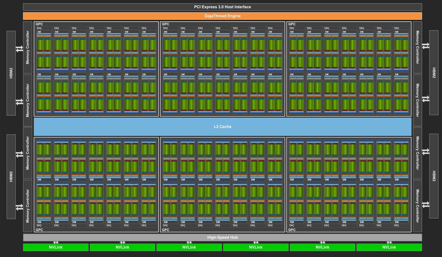
The Volta GV100 chip is organized into six regions, called GPU processing clusters (GPCs), each with two memory controllers and each with its own texture processing clusters (TPCs) and comprised of a bank of seven SMs. The GigaThread thread scheduling engine spans the whole shebang, which has a total of 84 SMs, adding up to:
- 5,376 32-bit integer cores
- 5,376 32-bit floating point cores
- 2,688 64-bit floating point cores, and
- 672 Tensor Cores
- 336 texture units
In the production Tesla V100 card, only 80 of the 84 SMs are activated; this means some of the SMs can be duds and the chip can still be used in production, which obviously increases the yield on the GV100 chips by a proportional amount. The clock speeds on the GV100s used in the NVLink-capable versions of the Tesla V100 cards were cranked up last fall, to 1.53 GHz with GPU Boost on, so the most recent performance numbers for this accelerator have inched up a tiny bit since the May launch last year; the PCI-Express versions are still running slightly slower and deliver slightly lower performance across integer, floating point, and Tensor Core units. The GV100 chip is not yet available in a form aimed at graphics cards or in other variants for Tesla accelerators – we mean akin to the P4 and P40 in the Pascal line, not the geared down versions of the GV100 that are used in the HGX form factor for hyperscalers or the PCI-Express version rather than the top-end SXM2 version that has NVLink support activated.
The capabilities of the seven latest GPUs used in the Tesla accelerator line – two each for Fermi and Kepler, and one each for Maxwell, Pascal, and Volta – are shown in the table below, with their chip maximums:
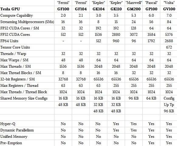
If some of the SMs are inactive, as is the case with the production GV100 chips so far, that proportion of the features drop and so does the performance. If all of the 84 SMs on the GV100 were activated, it would increase the performance by around 5 percent.
The Volta GPU compute engine has a lot going on; the entire kitchen sink of processing units and data sizes are available, including the 8-bit integer (INT8) instructions that came out with special versions of the Pascal chips aimed at machine learning inference, which were kept in the Volta design for compatibility reasons. The new Tensor Core 4x4x4 matrix math engines, which process in FP16 half precision and output in FP32 single precision, provide an amazing jump on machine learning training (about 12X over Pascal) and machine learning inference (about 6X). The question is, how do you keep all of those elements busy, which justifies putting them in there in the first place. No one wants dark silicon, and certainly not at these prices, but that said, everyone wants a compute engine that can do lots of different kinds of work and support various data types and processing methods, too.
“Pascal had this idea of paired operations, which had some constraints,” Jonah Alben, senior vice president of GPU engineering at Nvidia, tells The Next Platform. “In Volta, you can think of it as having an INT8 unit, an FP32 unit, an FP64 unit, a Tensor Core unit, and then there is the load/store path. Two of those can be kept full at any given time. In general, we issue one warp per clock, but in a partition there is only 16 elements of each of those things and once we issue to an instruction unit with that one warp per clock, it is now busy for two clocks and during the next clock you can do something else. Most importantly with Volta, you can now keep integer and floating point busy concurrently, whereas with previous designs any sort of addressing math or overhead that you were doing would steal cycles from the floating point.”
Another way of saying that is that with the Pascal GP100 GPU, inside of each SM you have two warp schedule partitions, and with the Volta GV100, there are four partitions, two each for floating point and two each for integer, and that gives enough throughput to do both kinds of calculations concurrently.
This is a very big deal, and Bryan Catanzaro, vice president of applied deep learning research at the company, who did a three year stint as a senior researcher at Chinese search engine giant Baidu before returning to Nvidia last fall, explains why this cornucopia of compute matters. Take a deep breath and let Catanzaro explain it in detail: “This is one of the things that I am really excited about because a lot of the future of AI is progressing towards what I would call funky models, in a sense that the memory addressing patterns are structured in more complex ways. When you are writing kernels to try to keep the GPU busy, the indexing math is something that you often have to spend a lot of time with to try to hide. As the access patterns get more interesting, that stuff gets harder to hide. I think the dedicated integer unit on Volta is going to help make it a lot easier to write machine learning kernels, and you will spend a lot less time trying to optimize that stuff away.”
Another big feature that is important for deep learning is forward progress guarantees for threads inside the same warp, even if they need to synchronize, which Tesla GPUs have not been able to do before. This, says Catanzaro, is going to enable a lot more interesting algorithms to be written against GPUs. And, he takes the time to tell us why: “A lot of code you could not write before because it could potentially hang the GPU is now possible thanks to the new threading model, especially for some sparser kinds of data analytics workloads. There are a lot of cases where we want to be collaborating between threads in more complicated ways, and Volta has a thread scheduler that can accommodate that. It is amazing to me that we could get more flexibility and more performance per watt. I was really concerned when I had heard that Nvidia was going to change the thread scheduler to be more flexible because I thought it would come at the expense of performance per watt. The reason that the older Pascal scheduler was not as flexible is that you get a lot of energy efficiency by ganging up threads together, and letting the threads be more independent had me worried about energy efficiency. But this actually got better.”
The reason it got better was because of the combination of architectural changes and process changes, but Alben says that the majority of the improvements here came from architecture. “This is a very large rewrite of the architecture, and the Tensor Core performance is obviously very large. But even if you look at Volta’s FP64, we are looking at 50 percent more performance in the same power budget as Pascal. The Volta SM is obviously a very ambitious design, and there are a lot of new elements in there.”
Volta has a completely different instruction set, and it is not just a Pascal GPU with Tensor Core thrown onto it, even if the block diagrams may suggest that in some way.
Don’t Forget The Memory
With any compute engine, memory capacity and memory bandwidth are important, and it is clear that Nvidia could add more HBM2 capacity to the Tesla Volta V100 package, and many had expected for the memory to be stacked eight high to double it up to 32 GB per unit. Nvidia had also hoped, many years back, that the Volta stacked memory would yield north of 1 TB/sec of memory bandwidth. As it turns out the Volta V100 package delivers 900 GB/sec of memory bandwidth, compared to the 720 GB/sec delivered with the first rev of HBM2 memory used in the Pascal P100 device. But the actual gap in memory performance is actually larger. On the STREAM Triad memory benchmark test, a Pascal P100 accelerator delivered 76 percent utilization of the peak bandwidth in the 16 GB of HBM memory on the device, or about 547 GB/sec; on the Volta V100 device, the STREAM Triad result was 95 percent of peak bandwidth, or 855 GB/sec. So at peak, the memory bandwidth improvement is only 25 percent, but if you look at sustained memory bandwidth, it is actually a 56 percent improvement.
To put it simply, the peak FP16, FP32, and FP64 performance all increased by about the same amount as the real-world memory bandwidth, which is a kind of balance and one that the HPC crowd could only reasonably expect. We don’t know how much of the real estate on the Volta GV100 is used up by the Tensor Core units, but let’s assume that it is a lot – enough that instead of 2X the raw performance using floating point units it was kept to only 50 percent more oomph here. That is a big piece of performance to give up, to be sure, but the machine learning training workloads needed a step function improvement, and Nvidia delivered it. And now, the HPC community can start wracking its brains to figure out how to port code from regular FP units to the Tensor Cores. When this is all said and done, future Tesla GPUs might only have Tensor Cores and look a whole lot like Google’s TPUs.
It is hard to say for sure, and fun to think about.
In any event, to keep those cores fed from that faster main memory required a complete reworking of the L1 and L2 cache memory on the chips. The L1 cache inside of an SM is four times faster on Volta than it was on Pascal, according to Alben, and it runs at the same speed as the L2 cache memory that is shared by the SMs. That L2 cache has a staggering 14 TB/sec of aggregate bandwidth, and now the L1 cache and shared memory look like a big address space; in the past, the L1 cache was implemented as a kind of scratch pad. But with them being merged, the effect is to make L1 cache look a lot bigger and to reduce the number of cache misses and the amount of programming tricks they need to do to manage data the data because, in effect, the shared L2 memory can look like L1 cache. It is the best of both worlds.
And ultimately, Nvidia split the difference and made a compute engine that was superior at both HPC and machine learning – a tough task indeed. We get the feeling that current and potential customers wish Voltas were more widely available, and less expensive, too. But the affect Volta will have on machine learning will be greater than it has on HPC, at least until HPC codes are rewritten to use Tensor Cores or become hybrid simulation and machine learning applications.
Catanzaro is philosophical and enthusiastic about how Volta will not just support machine learning, but transform it.
“One of the things that is great about machine learning is that it has algorithms and a way of thinking about the world that fits the technology that physics allows us to build now,” he explains, and once again, breathe in and listen here. “It is true that with Volta that we are providing an enormous number of new flops, and we are not providing 12X the bandwidth. What do I expect to happen with AI? People are going to try out models that they could not try before because they took a lot more flops. We know how to make our models more compute intensive, and in fact there is a lot of research that suggests that more intensive compute models get better results. Convolutions are in fact so compute intensive, and I expect that we will be seeing more convolutions. If you look at the inception blocks from Google, the things that they did in there were explicitly done to conserve flops at the expect of memory bandwidth. It will be interesting to see how that evolves. My personal expectation is that we are going to see architecture to shift a little bit to take advantage of the flops that we have. To a certain extent, this is like how things evolve, this is Darwinian pressure on the models, the architecture, and the manufacturing processes. We are all trying to make things better. There are certain things that are feasible and there are certain things that are not. In general, communication is always going to be harder to scale than computation. For the HPC people, it has been a long time since we had a byte per flops. We figured out things to do there, and with AI, there is tons of stuff that people will do. But it may shift a bit the way that people design their models.”
The Feeds And Speeds
At the moment, there are three Volta variants and five Pascal variants in the Tesla line, and here are the feeds and speeds of these devices:
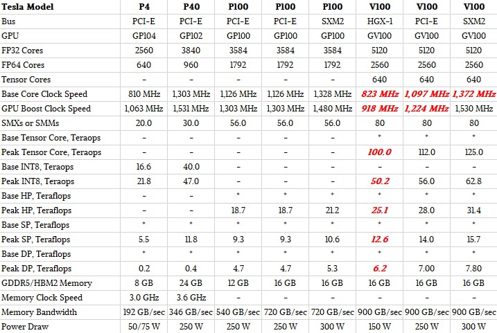
Items in the table shown in red are estimates made by The Next Platform. The precise feeds and speeds of the HGX-1 variant of the Volta GV100 card that is being adopted by the hyperscale community were not divulged – we expect to see more on this from Microsoft at the Open Compute Summit in March – and we have taken our best stab at what it might look like. We know that it is a 150 watt part, and that Nvidia says that it can deliver about 80 percent of the performance of the current top-end V100 SXM2 unit. As far as we know it has the same 16 GB of memory. The point is, the regular V100 unit delivers maximum performance per GPU, while the HGX-1 variant delivers maximum GPU aggregate performance per rack and maximum performance per watt. (And we also think the HGX-1 version offers lower cost per flops and ints, too, but we will talk about that separately.) Different customers optimize for different things.
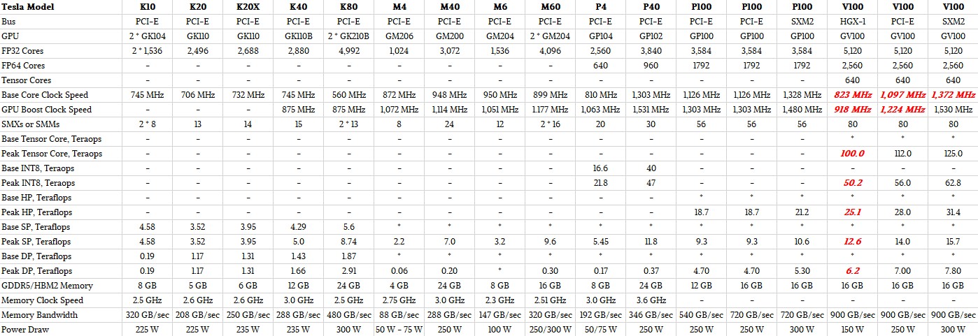
We have comparisons of the Nvidia GPUs all the way back through Maxwell and Kepler units, but that cannot fit onto one page. Click here if you want to bust your screen and look at that.
Next up, we will try to figure out the cost, the efficiency, and the bang for the buck of the various Tesla GPU accelerators. This is more black magic than we would like, and particularly so in a high demand environment where supply seems to be constrained a little.

CoreWeave’s 250,000-Strong GPU Fleet Undercuts The Big Clouds
CoreWeave, the upstart GPU cluster datacenter operator that was formerly a relatively small cryptocurrency miner based in Roseland, New Jersey, has filed its S-1 form with the US Securities and Exchange Commission to do an initial public offering. And that has a lot of people – those thinking of investing …
AMD Datacenter Sales Break Through $1 Billion In Q3
Here is a moment that Lisa Su, the chief executive officer who has lead the team that brought AMD back into the datacenter with the vigor the market needs, has been waiting six years for. In the third quarter ended in September, AMD’s datacenter CPU and GPU business broke through …
Why TSMC Did A $100 Billion Deal With Trump On US Chip Manufacturing
All presidents of these United States have the bully pulpit from which to lecture the American people and, for the past century, the rest of the world about how the global economy and culture should work. Donald Trump has certainly used this pulpit in his first and now second terms …
Be the first to comment