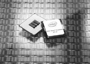
Intel is coming to the finish line with its 14 nanometer chip making process with the launch of the “Broadwell” generation of Xeon E7 server processors in China today.
Why China? Because for reasons that are not immediately obvious but are completely beneficial to Intel, the Chinese market has for the past several years been adopting four-socket servers in large scale datacenters at a rate that is considerably higher than their peers in the rest of the world. These new Xeon E7 v4 processors will be a big hit for big iron there and anywhere else where having a big shared memory for applications is key.
The Broadwell Xeon E7 v4 chips are the penultimate chips in the Broadwell generation, with Intel expecting to finish off the rollout of server chips in the 14 nanometer generation that began a year ago with Xeon E3 chips. Intel still has a Xeon E5-4600 v4 to get into the field for two-socket and four-socket systems, and is expected to do so shortly.
The launch of the “Broadwell-EX” processors, as the Xeon E7 v4 chips are known internally at Intel, doesn’t just mark the end of the “Brickland” server platform has spanned that past three generations of Xeon E7 chips (including the “Ivy Bridge” variants from February 2014 and the “Haswell” versions from May 2015), but quite possibly a distinct Xeon E7 product line at all from Intel. According to the specs that we reported on last year about the future “Skylake” Xeons due in 2017, the future “Purley” platform and what looks like a single family of Skylake Xeons will be available for machines with two, four, or eight sockets. So the line between a Xeon E5 and a Xeon E7, at least in marketing and unique sockets, looks to be going away.
This stands to reason, given that Intel has offered special variants of the Xeon E5 that scale up to four sockets (the E5-4600 series) and used to sell special versions of the Xeon E7s that scale down to two sockets (the E7-2800s). With the company having to offer more and more SKUs within each family to meet the special needs of hyperscalers, ODMs, and OEMs, Intel probably wants to eliminate some of the complexity in its line. It looks like some variants will have two UltraPath Interconnect (UPI) ports per socket, the same number of QuickPath Interconnect (QPI) ports that the Xeon E5-2600 and E5-4600 processors have, and others will have three UPI ports per socket, like the Xeon E7-4800 and E7-8800 processors have.
The number of ports determines how many sockets can be glued together and the number of hops between processors, and there are varying topologies to accomplish this. Two QPI or UPI ports gives a perfect balance between two sockets and two links between sockets, which allows for super-efficient NUMA scaling, and three QPI or UPI ports allows an all-to-all connection between four sockets with half the bandwidth and still reasonably good scaling. You can scale to four sockets with the Xeons with two QPI or UPI ports per socket, but a third of the time you will have to make two hops, which introduces NUMA memory latencies. With an eight-socket configuration using chips with three QPI or UPI links, you have to make two hops half the time on average with the NUMA topology.
By unifying the Xeon E5 and E7 sockets but allowing for different UPI links, Intel can provide all of the benefits of the diversity of the Xeon line without having to make OEMs and ODMs create distinct motherboards. This may have an adverse effect on profits, given what Intel charges for Xeon E7 chips, but it will also reduce the friction on four-socket and eight-socket processor sales – something that is important in a world where certain workloads want larger and large chunks of main memory as the Xeon E7 has historically offered.
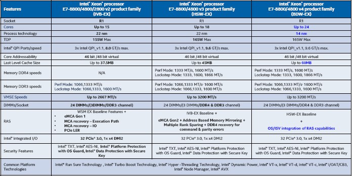
There never was a “Sandy Bridge-EX” Xeon E7 version put in the market, which was mothballed so Intel could close the gap between the E5 and E7 processor launches as it entered the Ivy Bridge era several years ago. With those Ivy Bridge-EX chips in 2014, Intel had plenty of pent-up demand since it had been a long time since the “Westmere-EX” Xeon E7 chips were launched in April 2011. The Ivy Bridge Xeon E7s had up to 15 cores, a 50 percent increase over the Westmere-EXs, and offered up to 6 TB of main memory in a four-socket system and up to 12 TB in an eight-socket machine. These were pretty beefy machines, and came to market just as in-memory processing was getting set to take off.
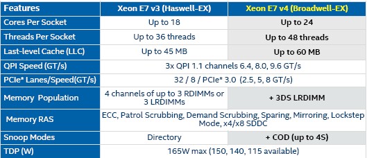
With the Haswell-EX chips from 2014, the memory, the cores saw lots of microarchitecture improvement, Intel boosted to top bin core count to 18 cores (up 20 percent) and L3 cache to 45 MB (up 20 percent), and the QPI links were revved to 9.6 GT/sec (also up 20 percent). The clock speeds dropped, as they often do as Intel adds cores, so the performance improvements in the jump from Ivy Bridge-EX to Haswell-EX really depending on the nature of the workloads. Integer math performance was around 20 percent to 30 percent across SKUs, and transaction processing performance was generally up by between 40 percent and 50 percent. On average, across diverse workloads, a four-socket Haswell-EX machine provided about 40 percent more oomph, with floating point processing due to AXV2 pulling up the class average bigtime.
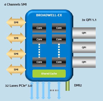
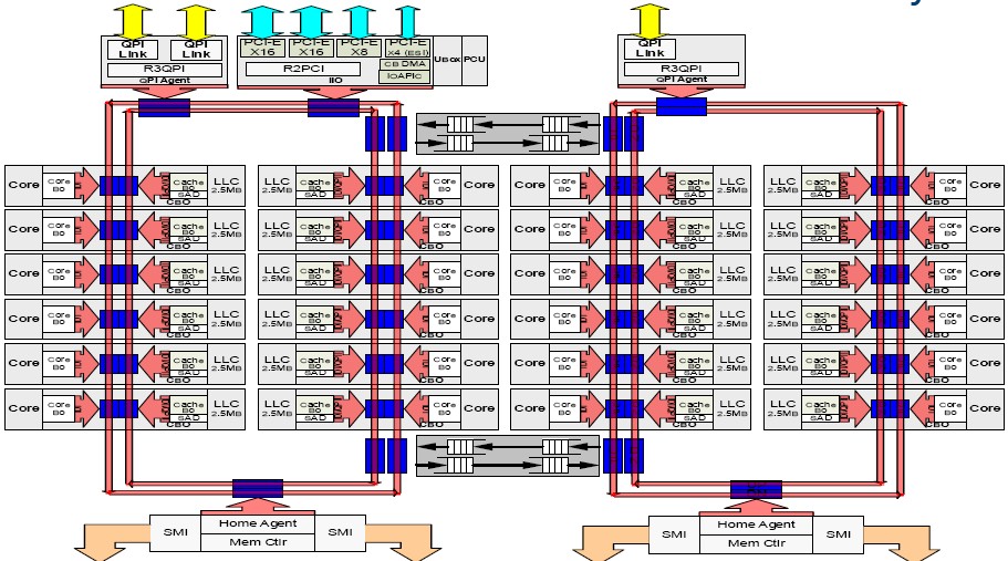
With the Broadwell-EX Xeon E7 chips, Intel is sticking with the same Brickland platform but it is doubling up the memory capacity using 128 GB DDR4 memory sticks based on 3DS LRDIMM form factors, which yields up to 12 TB on a four-socket setup and up to 24 TB on an eight-socket setup. As with prior EX variants, the Broadwell-EX processors have four Scalable Memory Interconnect (SMI) ports that link the on-die memory controllers to “Jordan Creek” buffer chips out on the memory cards stuffed to the gills with DDR4 DIMMs.
We think it is unlikely that many customers will buy 128 GB memory sticks, especially if they carry the kind of premium that 64 GB sticks did when 8 GB, 16 GB, and 32 GB memory were more common on EX-class systems.
In general, the Broadwell Xeon E7s are exactly what you expect from a process shrink from Intel. There are a bunch of nips and tucks. With the Broadwell-EX, the top bin core count has gone up by 33 percent and so has the L3 cache memory, and the clock speeds are the same or down a smidgen, but the QPI links are running at the same speed. (We will get into the specifics of the memory subsystem changes in a minute.)
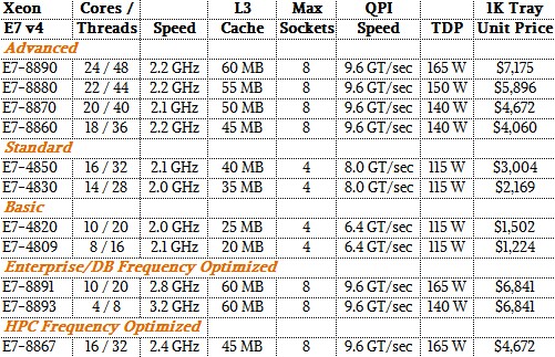
As it turns out, the SKUs are almost perfectly mapped from the Haswell Xeon E7s to the Broadwell E7s, and the prices for the chips are exactly the same, which means the price/performance change is mathematically identical to the performance change, SKU to SKU. As in Xeon E7s from past years, there are Basic, Standard, and Advanced Editions of the processors which have increasing core counts and cache sizes within each Xeon E7 family as well as higher thermal design points and higher prices. (You pay for performance in heat and dollars, because these are the laws of physics interplaying with the laws of economics.) The Basic and Standard editions of the Xeon E7s are used for four-socket servers, while the Advanced versions are for machines with eight-sockets. This NUMA functionality is provided by Intel gluelessly, meaning there are no external node controllers needed to provide the NUMA links. It is all done on-chip over QPI links. For machines with more than eight sockets, you have to go to a vendor that has its own NUMA controllers and that speaks QPI (as Hewlett-Packard Enterprise and SGI do).
In addition to these three Xeon E7 variants, Intel also has a special SKU for high performance computing, which has a relatively high core count, a modestly large cache, scalability to eight sockets, and a relatively low price. Intel also has an Enterprise/Database variant that has lower core counts, higher clock speeds, and larger caches than the Standard parts and as large as the top-bin advanced part. The idea here is that databases are priced on a per-core basis, so increasing throughput and reducing the number of cores can have a big impact on overall system price. (The database software is often many times more expensive than the hardware on big iron.)
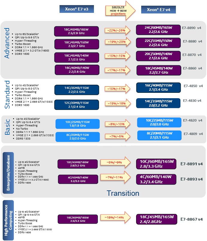
Here is how the Haswell Xeon E7 SKUs line up against the Broadwell Xeon E7 SKUs:
In the chart above, the performance increases SKU-to-SKU are for SPECint_rate_2006 integer math benchmark (SIR) and for a HammerDB online transaction processing test (OLTP). The base and Turbo Boost clock rates are shown with each chip SKU, as are the core counts, L3 cache size, and power dissipation. These two tests, by the way, are among a handful that Intel uses to gauge the relative performance of its Xeon E7s, and we will be doing a follow-up story on Xeon E7 performance that gets into these in detail across the generations.
What is immediately obvious from the chart above is that the big performance boost for these two workloads is coming from the chips that have the core count and L3 cache increases; the Basic chips, which only have a 100 MHz boost in clock speed, are showing much more modest performance increases, reflective of only the architectural differences between the Haswell and Broadwell cores, for the most part. Ditto for the database SKUs, which have the same base clock speeds and only 100 MHz more on Turbo Boost as well as identical core counts and only the 33 percent larger cache. And the HPC variant has two more cores, the same L3 cache, and a slightly lower clock speed for a performance that is more in line with the top-bin parts but not quite there. (We will get LINPACK floating point numbers to see how that has changed.)
In general, as we have pointed out before, the Broadwell core provides about 5.5 percent more instructions per clock than the Haswell core, which itself was 10.5 percent better on IPC than the Ivy Bridge core.
The one chip that did not make the cut from the Haswell Xeon E7s to the Broadwell Xeon E7s was the 18-core E7-8880L, a low voltage variant of the Haswell-EX that ran 20 percent slower than the regular E7-8880 and dropped its power draw by 30 percent to 115 watts from the 165 watts of the plain vanilla part.
Here are the basic feeds and speeds of the eleven new Xeon E7 v4 processors:
All of the tweaks that Intel made with the Broadwell cores in the Xeon E5 processors to make virtualization run more efficiently or for cache or main memory to be allocated to cores in a more efficient way move over to the Xeon E7 v4 chips. Another technology that is moving over is called Cluster On Die, or COD.
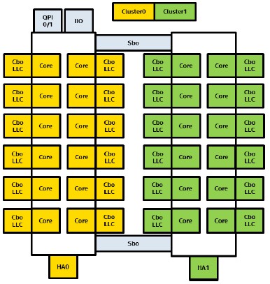
The idea with COD, which was introduced with the Haswell Xeon E5 chips in September 2014, is to slice a chip with high core counts and a large L3 cache into two and treat them a bit like an on-chip, two-socket NUMA server. By doing this, operating systems and applications can create NUMA domains for each half of the chip and try to make sure data and processing stay on each of the two loops that comprise the Xeon E7 chip. This does two things. First, the access latency to the L3 cache segments is lower for any half of the chip, and moreover, the memory controller only has to check one half of the chip where it has control of threads and is therefore more likely to hit open pages in the memory controller.
With the Haswell Xeon E5s, the COD feature was only supported in two-socket systems, but with the Broadwell Xeon E7s, it now works on four-socket machines. (It has not been extended to eight-socket machines, and probably will not be until the Skylake generation, and maybe not even then.) It is not clear how much of a performance boost COD offers, but on benchmark tests stressing memory bandwidth, a 24-core E7-8890 v2 running at 2.2 GHz with 1.6 GHz DDR4 memory with two DIMMs per channel was able to drive 347 GB/sec of memory bandwidth on a 100 percent read test compared with 334 GB/sec with COD turned off. With a 50 percent read/write mix, the COD boost was not as large, 305 GB/sec with it on and 297 GB/sec with it off.
The Xeon E7 v4 chips are available now, and will be soon appearing in systems from all the usual suspects. We will be looking into these machines and also doing a detailed analysis on the performance and price/performance of the Broadwell-EX compared to prior generations and alternatives in the market for big iron. Stay tuned.



Nice article, but I think its important to mention the 70+ RAS features that E7 has above and beyond E5, things like Machine Check Architecture and DDDC+1 are fairly easy to explain and are key drivers behind the success E7 is having at replacing the legacy RISC platforms.
I view it more as evidence the previous E7 models are deficient as compared to the latest gen. Every new generation seems to be announced with each significant features seemingly to indicate they are woefully behind yet still claim they are gaining parity with RISC. By the way, The only RISC left is SPARC & IBM POWER. SPARC is not relevant and the only viable alternative to Intel is IBM Power. Said another way, Intel E5 and E7 processors not only do not have parity with RISC (IBM Power) but customers do not see how deficient each Intel generation is until the next is released (largely due to an impressive marketing machine). Furthermore, we often hear of all these RAS features yet lacking a detailed description of each, for which models they are available and which they are not as Intel has a history of claiming a feature only for it to NOT apply to all or even most of that generation of chips.
This is sillly. Intel claims 27 new world records for the Intel E7 v4. Here are links to all Intel benchmarks:
http://www.intel.com/content/www/us/en/benchmarks/server/xeon-e7-v4/xeon-e7-v4-world-record.html
So, let us look at an Intel “world record”. Take for instance SPECint2006. Intel 4-socket E7v4 gets 3,570 points which is not too shabby:
http://www.intel.com/content/www/us/en/benchmarks/server/xeon-e7-v4/xeon-e7-v4-general-compute.html
That is 893 points per E7v4 cpu. But one single Oracle SPARC M7 cpu gets 1200 points. That is 1.34x faster:
https://blogs.oracle.com/BestPerf/entry/201510_specpu2006_t7_1
And SPARC M7 is built to scale-up. Intel E7v4 is not, it stops only at 8-sockets.
Lets look at the Intel SPECjbb2015 “world record”. Intel 4-socket E7v4 gets 219,300 points. That is 54,800 points per E7 cpu. But one single SPARC M7 cpu gets 120.600 points, that is 2.2x faster:
https://blogs.oracle.com/BestPerf/entry/201511_specjbb2015_t7_1
Lets look at the Intel SAP “world record”. Intel 4-socket E7v4 gets 41,450 users:
http://www.intel.com/content/www/us/en/benchmarks/server/xeon-e7-v4/xeon-e7-v4-business-processing.html
That is 10,362 users per E7v4 cpu. But two SPARC M7 cpus get 30.800 users, that is 15.400 users per M7 cpu. That is 1,5x faster
https://blogs.oracle.com/BestPerf/entry/20151025_sap_sd2tier_t7_2
Look at SPECvirt2013 on the same site. Intel 4-socket E7v4 claim 4,231@237 VMs. Two SPARC M7 gets 3,198@179VMs, that is 1.5x more points.
I could go on and on. I dont understand why Intel lie about they have 27 world records? SPARC M7 is typically 2-3x faster than IBM POWER8 and Intel E5-2699v3, all they way up to 11x faster on database loads. And, encryption is free on SPARC M7, you loose 1-3% performance with full encryption. If you enable encryption on x86, watch performance drop to one third or worse.
On this site are 30ish TRUE world records. All by SPARC M7 from last year. Oracle is working on their SPARC M8, which again, will be more than twice as fast as the current generation, i.e. SPARC M7. Intel only gets 10-15% performance increase every generation.
https://blogs.oracle.com/BestPerf/entry/20160531_sparc_m7_8_sap