

For the past five years or so, there has been a lot of talk about accelerated computing being the new normal and about the era of the general purpose processor being over in the datacenter, and for good reason. We have run out of ways to do all of the complex processing our applications require on a single device in a power and cost efficient manner.
Only last week, we did a thought experiment about how we should have streamlined chiplets for very specific purposes, woven together inside of a single package or across sockets and nodes, co-designed to specifically run very precise workflows because any general purpose processor – mixing elements of CPUs, GPUs, TPUs, NNPs, and FPGAs – would be suboptimal on all fronts except volume economics. We think that this extreme co-design for datacenter compute is the way the world will ultimately go, and we are just getting the chiplet architectures and interconnects together to make this happen.
Radoslav Danilak, co-founder and chief executive officer of processor upstart Tachyum, is having absolutely none of that. And in fact, the Prodigy “universal processor” that Tachyum has designed is going in exactly in the opposite direction.
Danilak says that fixing the bloat and wiring issues in modern processor designs that allows for a self-contained, complete, integrated processor, which he argues can do the kind of work that we have argued requires a series fast integer CPU engines, GPU or FPGA floating point engines, and NNP matrix math engines all lashed together with high speed interconnects that span sockets and boxes. (But don’t call it a hybrid chip, because Tachyum will argue with you about that.) And while we still think that locking down compute components in fixed proportions in a single chip that gets updated every two to three years – forcing them to advance at the same pace – is as risky as trying to package collections of chiplet compute units of different styles and capacities, we also admire the elegance of what Danilak and co-founders Rod Mullendore, chief architect, and Igor Shevlyakov, vice president of software, have designed and the ambition they bring to datacenter compute.
Another Upstart Chip Startup
It takes a certain amount of ego, and lots of practical experience, to launch a new processor in the second decade of the 21st century. This is a tough market, and we have seen a proliferation of compute devices that is a joy to behold. But not everyone is going to make it, as is always the case. Luckily, there is venture funding to burn and people willing to make bets on the people able to design something new.
Tachyum, which is headquartered in Santa Clara, California with a development lab in Bratislava, Slovakia, has plenty of seasoned engineers and executives on its team. Danilak designed his own Very Long Instruction Word (VLIW) processor back in the early dot-com boom era and a few years later created an out of order execution X86 processor with 64-bit processing and memory for a company called Gizmo Technology (we have never heard of his chip) and then did a stint at Toshiba as the chief architect of the Toshiba 7901 chip, a variant of the MIPS R5900 Emotion Engine processor used in the PlayStation2 game console and presumably used in various Toshiba microcontrollers and electronics. Danilak did a one year project at Nishan Systems creating a single-chip network processing unit (NPU) that consolidated down the functions of 20 different chips, and then was a senior architect at Nvidia designing the features of the nForce 4 GPUs and the “Fermi” first generation Tesla GPU accelerators. After leaving Nvidia in 2007, just as the GPU acceleration wave was getting set to take off, Danilak found flash storage maker SandForce and created its homegrown flash controller; SandForce was sold in 2010 to LSI Logic for $377 million. After that, Danilak co-founded Skyera, a maker of all-flash arrays that Western Digital acquired for an undisclosed sum in the summer of 2015, and bopped around looking for new ideas for a year before co-founding Tachyum in September 2016 with Mullendore and Igor Shevlyakov.
It takes a team to create a processor, the software stack for it, and to get it out the door to prospective clients, and the Tachyum team is pretty experienced at this. Mullendore was a senior architecture engineer at Nishan Systems during and after the dot-com boom, and then did some work for McData, a maker of storage area network switches when it was part of EMC and then when it was sold to Brocade Communications, where he remained for a while after the acquisition. Mullendore then took the job of principal architecture engineer at SandForce, and then he followed Danilak to Skyera and now Tachyum.
Shevlyakov, the other co-founder of Tachyum, started out in the early 1990s as a software engineer and then focused on compilers at a number of startups in Russia during the beginning of the dot-com boom, and at its peak, between 1999 and 2001, was a senior compiler engineer at real-time operating system maker Wind River. Shevlyakov then spent more than a dozen years at MicroUnity, which had developed a RISC/SIMD processor called BroadMX aimed at network processing jobs, where he ported the GNU open source toolchain to the processor. He joined up with Danilak and Mullendore at Skyera, where he ported the GNU toolchain to the proprietary chip the company created to control flash as well as working on the flash translation layer in its all-flash arrays. After Western Digital acquired Skyera, Shevlyakov stuck with his co-founders and took charge of the software stack at Tachyum.
Ken Wagner, vice president of business development, is also a co-founder and has worked for a number of silicon startups, and Kiran Malwankar, who founded scale-out storage maker Pavilion Data Systems, is vice president of systems engineering. Fred Weber, who was a co-founder of supercomputer makers Encore Computer and Kendall Square and who was chief technology officer at AMD and helped create the 64-bit Athlon and Opteron architectures, is an advisor, and so is Steve Furber, professor of computer science at the University of Manchester and, in the 1980s, designed the first 32-bit Acorn RISC Machines processor that we know as Arm. Christos Kozyrakis, an expert in distributed systems often affiliated with Google and a professor at Stanford University, is also an advisor.
Coming Down To The Wire
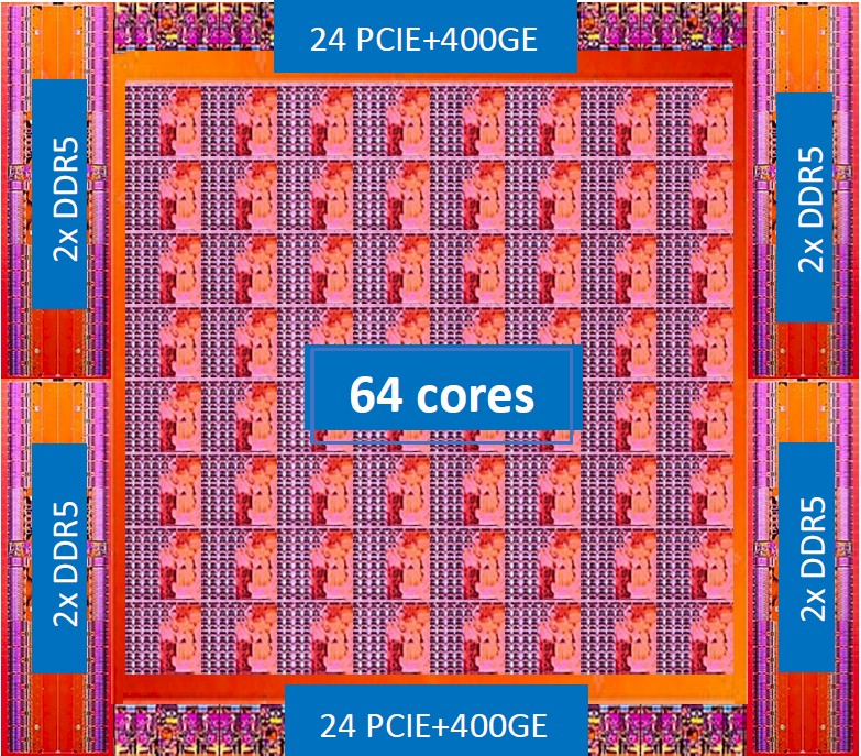
The Prodigy chip has been in design for several years, and the company has an internal System C simulator available for internal development and benchmarking uses. An FPGA hardware emulator will be available in the fall for research, as they move towards tape out at the end of the year. (It has been delayed several times, but that is normal for chips in general and first generation chips in particular.) It is, like so many advanced chips these days, etched using the 7 nanometer processes of Taiwan Semiconductor Manufacturing Corp. And that advanced manufacturing allows it to cram a lot of components into the 290 square millimeter device.
Interestingly, the design is the result of an intense focus on the wires connecting blocks of circuitry together, and then putting together what Tachyum thinks is the right ratio of components to appeal to hyperscalers, HPC centers, and machine learning and inferencing farms. The issue, says Danilak, is that wires are getting slower. Here are some familiar charts: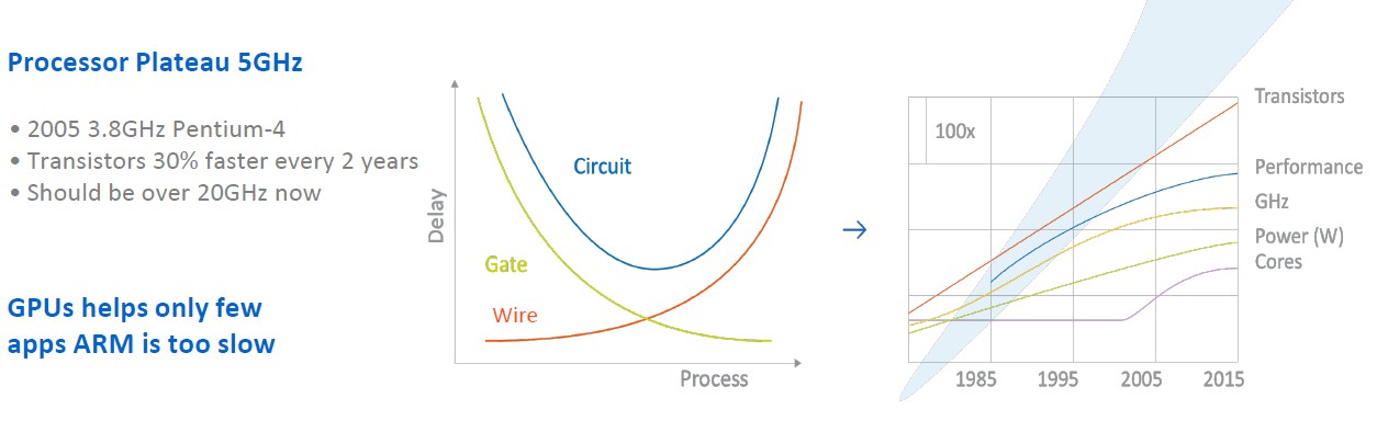 “We have a performance plateau around the clock speed and the performance per core is not growing that much,” Danilak tells The Next Platform. “The core counts are growing, but we are also decelerating the clock speed because of thermal issues. All of the transistors are faster, but the problem is that the wires become thinner and thinner and more resistive, and wire delays are therefore increasing. There used to be a 100 picosecond per millimeter delay in chips, and now is it more like a 1,000 picosecond per millimeter delay.”
That wire resistance creates heat, of course, but also latency, so the trick, according to Danilak, is to keep the wires as short as possible. That way you can clock chips faster than you might otherwise and also you reduce the total time of computation – the time to get the data plus the time to crunch it – and get more work done. The trick is to extract out parallelism in the workload running on the chip that makes the wire delay in the computational time (much as the cache hierarchy masks computational latency in standard processors), and that requires some clever compiler work – hence, Shevlyakov, who has such deep compiler experience.
So without further ado, here is the die shot of the Prodigy chip:
Danilak makes a bold claim: “Every core is faster than a Xeon core or an Epyc core, and it is smaller than an Arm core, and overall, our chip is faster than a GPU on HPC and AI.”
We have to split hairs on what the definition of “fast” means in that sentence, but clearly, with Tachyum pushing up the clock speed to 4 GHz on the Prodigy-1 chip, that is considerably faster than the top bin parts out of Intel, AMD, Ampere Computing, and Marvell and on par with the fastest chips IBM can make in its Power9 line.
The Prodigy chip is using standard cells and SRAMs from TSMC using its 7 nanometer FinFET processes, which have 12 metal layers and operates at 0.825 volts.
The processor pipeline has its out of order execution handled by the compiler, not by hardware, so there is some debate about whether this is an in order or out of order processor. Danilak says that instruction parallelism in the Prodigy chip is extracted using poison bits, which was popular with the Itanium chip which this core resembles in some ways and which are also used in Nvidia GPUs. The Prodigy instruction set as 32 integer registers at 64-bits and 32 vector registers that can be 256 bits or 512 bits wide, plus seven vector mask registers. The explicit parallelism (again, echoes of Itanium) is extracted by the compiler and instructions are bundled up in sizes of 3, 8, 12, or 16 bytes. The pipeline can do two loads, two multiply-adds, one store, one address increment, one compare, and one branch per cycle – that’s eight RISC-y micro-ops per cycle and this averages out to 1.72 instructions per cycle – about what we think a “Skylake” Xeon SP core can do, and Tachyum actually cites our data, derived from information pieced together on IPC from Intel over the years, in its own charts. (You’re welcome.)
The 64 cores are laid out in four redundant blocks of 16 cores, all linked by a mesh interconnect through their L3 caches; memory controllers are linked to the cores on a separate mesh interconnect from the caches to avoid congestion on the meshes. Each quad has a pair of memory controllers that will support either the DDR4 or DDR5 memory protocols as well as 18 lanes of PCI-Express 5.0 peripheral interconnect implemented in SerDes. In the typical configuration, those SerDes will be used to implement a single PCI-Express 5.0 x16 per quad plus a pair of 400 Gb/sec Ethernet controllers, but the configuration is flexible. There is an option to add HBM3 memory to these chips, which is expected for the high-end of the product line aimed at HPC and AI workloads with higher memory bandwidth needs than can be met with DDR4 or even DDR5. But don’t think this will be the mainstream Prodigy part, or that it will be cheap.
Danilak says that with eight channels of DDR5 memory, current HBM2 memory will only deliver about 2X higher memory bandwidth and it is much more of a hassle. “The bandwidth is in comparable territory,” which is exactly what IBM is saying about the souped-up DDR4 and DDR5 memory coming with the Power9’ and Power10 processor.
Now, let’s drill down into the Prodigy core:
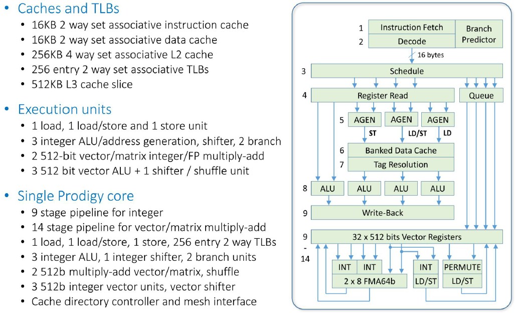
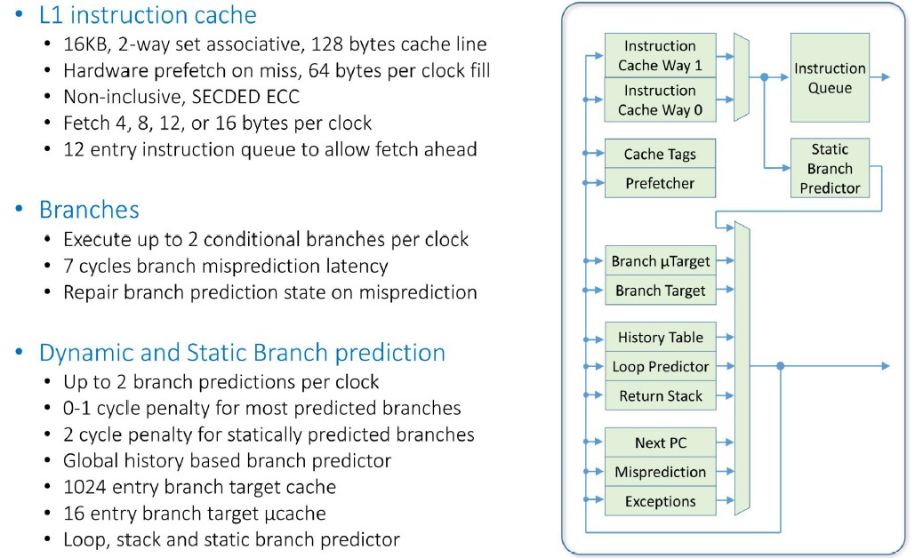
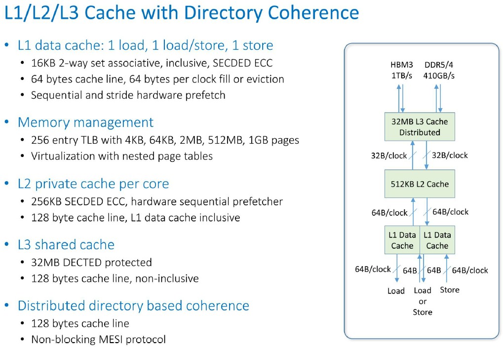
The L1 caches are a bit small compared to other core designs, at 16 KB for data and 16 KB for instructions, but the 256 KB L2 cache on the core and the 512 KB slice of L3 cache also on the core (which weaves together to create a giant 32 MB shared L3 cache for the entire die) is perfectly normal. As you can see, the integer pipeline is nine stages deep and the vector pipeline adds another five stages.
Now let’s get out the gorpy details for those of you who love this stuff. Here is how the Prodigy core deals with instruction fetching:
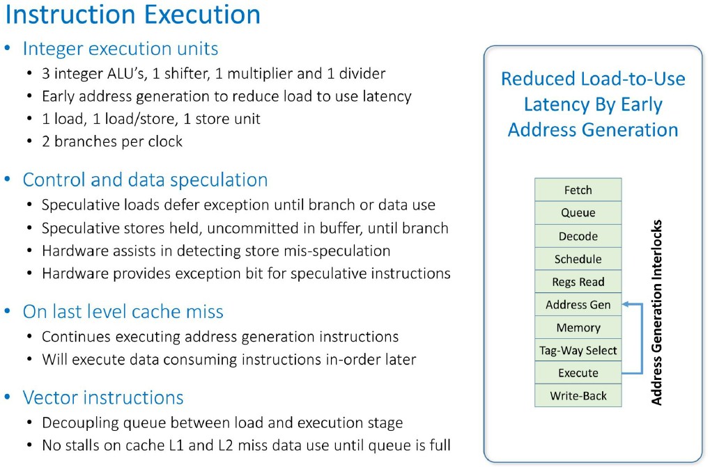
And here is the flow for instruction execution:
This is the Prodigy chip cache hierarchy in action:
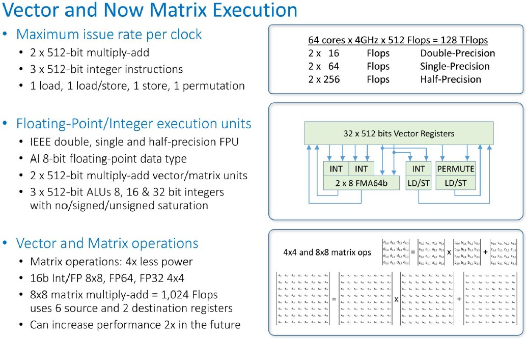
And this is how the vector and matrix math units lay out and work:
A couple of things pop out to our eyes in these charts.
On the links out to the DDR5 and HBM3 memory out of the L3 cache, the aggregate bandwidth is 410 GB/sec into and out of the DDR5 memory and 1 TB/sec into and out of the HBM3 memory. You have to really need 2X the bandwidth to pay extra for the HBM3 – and there are many AI and HPC workloads that will benefit from these since they are largely constrained on memory bandwidth, not compute – which is why we shard up these applications and throw them across so many server nodes.
The vector units will support normal double precision 64-bit FP64 and single precision 32-bit FP32 operations, plus half-precision 16-bit FP16 as well as 16-bit bfloat16 (invented by Google) as well as 8-bit floating point (a proprietary format invented by Tachyum). The vector units also support INT8, INT16, and INT32 integer operations. There are also matrix operations that can be deployed on these vector units, allowing 4×4 matrix multiply operations on FP32 and FP64 data and 8×8 matrix multiply operations that can be run on either 16-bit or 8-bit integer or floating point data. This double duty of the vectors is very interesting indeed, and Tachyum hints that it can double up the performance in a future processor. We need to get our heads wrapped around this a little better, but it looks like the four 512-bit SIMD units can operate as vectors or tensor cores, depending on the need, and that frees up die area for these two different ways of doing math. The “Volta” and “Turing” GPUs from Nvidia have different kinds and numbers of integer, floating point, and tensor core units, by contrast.
To Danilak’s way of thinking, floating point multiply-add units are essentially the same – it’s not like Nvidia knows how to do this better than anyone else, he says. GPUs run at 1.3 GHz to 1.5 GHz and CPU multiply-add units running at 2.5 GHz to 3 GHz to sometimes 4 GHz are delivering essentially the same performance. Everyone is on TSMC 7 nanometers, except Intel which is ramping up its 10 nanometer equivalent for this year. There will be no real process advantage that is sustainable.
“Where CPUs, GPUs, and TPUs they different is in the control and the amortization of the power for computation.” To simplify a bit, the argument is that warp has 32 threads running at about half to the third of the speed of an AVX2 vector unit in a Xeon chip, which can do four “threads” of floating point at about a third to a quarter of the power consumption. The X86 chip has very expensive branch prediction and the decoding is very complicated. All of this adds to power but yields better performance than for previous X86 chip generations, but at a cost of constantly reducing clock speeds and increasing threading. You can move to AVX-512 and have vectors that are twice as wide, but you have to move slower. The idea with the Prodigy chip is to have an architecture that is somewhere between the CPU and the GPU, taking out all of the legacy stuff and shortening all of the wires between the cores and other elements as much as possible to reduce latency, boost clock and mesh fabric speeds on the die, and get higher throughout and, presumably, better bang for the buck.
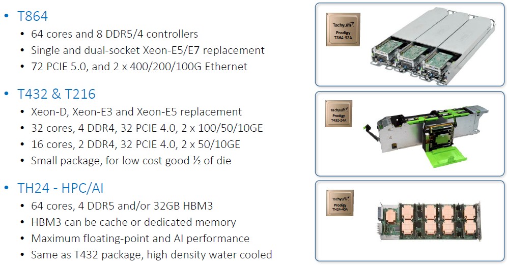
Here is what the Prodigy “universal processor” family’s initial SKUs will look like:
Tachyum had been hoping to sample the Prodigy chip in late 2019, but it was delayed for a few months and is just getting going now. The company was expected to have volume shipments in products towards the end of 2020, but now the plan is to get it into systems and into the field in the second half of 2021, including a four-socket system that will go into Open Compute Project racks. The plan was to launch a two-processor machine with 128 cores with four stacks of HBM in Q1 2020, then a single chip with 64 cores with eight DDR4 memory controllers in Q2 2020, and then a 32 core chip with four DDR4 memory controllers in Q3 2020. It’s unclear if this is still the rollout cadence, but the timing has clearly been pushed out.
Tachyum has not set pricing yet, but has some ideas. Danilak says that the standard DDR4/DDR5 Prodigy SKUs will cost a few hundreds of dollars to a few thousand dollars, and the high-end one with the 32 GB of HBM3 memory is expected to cost under $10,000, delivering 3X better price/performance (speaking very generally) than CPU or GPU alternatives.

Replacement means that it’s compatible with Xeon socket?
I highly doubt that. Replacement means function, not form.
to be used in the next Mac Pro;)
“as well as 18 lanes of PCI-Express 5.0 peripheral interconnect implemented in SerDes”
It’s all SerDes all the way down as far as most links are concerned and it’s just some protocol controller logic on top of the SerDes that’s doing the PCIe/other protocol business. Now who has the best SerDes IP that’s what I want to know and there are several third party SerDes IP providers but some processor makers user their own.
SerDes across clock domains is harder among other sorts of things but some folk’s special sauce make for less latency than others.
That was quick. For a moment I was wondering if the Mill project had done a name change, but these seem to be a whole lot more conventional RISC style.
How interesting to get both this and hopefully Mill in a near future.
We will look into that one, too.
It is claimed that “every core is faster than a Xeon core or an Epyc core” using which metrics for which workloads comparing with which generations of Xeon and Epyc CPUs?
Where are SPEC CPU2017 estimates or similar standard results?
So it’s QEMU’s ability to run x86, RISC-V, ARM, etc. binaries on Prodigy. Somehow false marketing by Tachyum to state “all run in Prodigy”.