
Qualcomm had datacenter envy back when Intel ruled the bit barns of the world, and now it has it even worse now that Nvidia has shown how AI processing can utterly transform the finances of a chip maker. Qualcomm is also the volume leader for high-end Arm CPUs and add-on circuits for smartphones, and it has the IP and the talent to create server CPUs and AI accelerators that can take a piece of the enormous AI inference opportunity.
What it doesn’t have is a technology that is going to take much of a bite out of Nvidia’s AI inference workload, no matter how excited Wall Street is about that prospect this week as Saudi Arabia’s Humain AI startup has emerged as a sugar daddy for Qualcomm’s datacenter AI ambitions. And Qualcomm has absolutely no shot of creating anything that can take on Nvidia in AI training, which is where Nvidia will make around half of its $183.5 billion in datacenter revenues in fiscal 2026 ending in January according to our model.
This is the green-tinted lens through which you have to look at the deal with Humain that Qualcomm outlined a little bit more this week.
Back in May, Qualcomm inked a memorandum of understanding with Humain to collaborate on the development of AI technologies at the edge and in the datacenter. That MOU not only included the expected AI chips for inference – we wish they had a better product name and we wish we knew the code name – but edge devices powered by Snapdragon and Dragonwing system-on-chip designs that aim to “accelerate” back-end cloud infrastructure and to tune up Humain’s Arabic large language models for these SoCs. And significantly, the MOU called for Qualcomm to “develop and supply state-of-the-art datacenter CPU and AI solutions,” which unequivocally means that Qualcomm is getting back into the server CPU business while also getting funding to expand its AI accelerator lineup.
Let’s tackle the AI accelerators first, and then ponder the server CPUs after that.
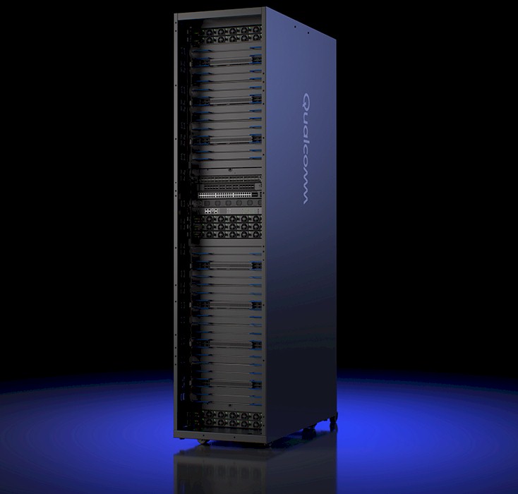
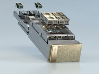
Concurrent with the Future Investment Initiative 2025 conference in Riyadh, Saudi Arabia this week, Humain and Qualcomm moved from an MOU to an actual contract, and revealed that two future AI accelerators were in development with Humain as the first customer. Like Broadcom with at least two of its XPU customers, Qualcomm is also providing Humain with complete rackscale systems, not just chips that it has to provide to an original design manufacturer like Quanta, Foxconn, Invensys, Jabil Circuit, Celestica, or WiWynn (just to name a few biggies) to turn into servers and cluster into systems.
The original AI 100 XPUs from Qualcomm were announced way back in 2019 and shipped sometime in the first half of 2021. The only time we ever saw them was before waferscale system supplier Cerebras Systems had tweaked its software stack so it could do inference. But in March 2024, when the WS-3 compute engines and their CS-3 systems debuted, Cerebras was offloading inference to racks of AI 100 accelerators from Qualcomm to do inference cheaper than could be done at the time with its own systems. By September last year, Cerebras had tweaked its software to run inference workloads, and we never heard about the AI 100 XPUs again.
Frankly, there are so many startups chasing AI inference and there was so much going on we never did circle back. (Apologies for that, Qualcomm.) In any event, Qualcomm published a series of benchmarks on the AI 100 accelerator back in September 2021, which is interesting reading and which showed these devices standing toe-to-toe with low-end and high-end Nvidia “Ampere” GPUs and other inference engines suitable for the edge on ResNet-50 image processing tests. The AI 100 did particularly well on inference per second per watt compared to Nvidia A100 GPUs, which is an important fact.
But inference has moved on, and in a big way, with GenAI, and the compute workload has gotten a lot more intense. But so has the desire to find a cheaper alternative – should one really exist – compared to running mixture of expert, reasoning inference on Nvidia rackscale CPU-GPU hybrids.
In October 2024 – and we cannot find an exact announcement date, which is peculiar – Qualcomm started shipped geared-down versions of the AI 100 called the AI 80 and also created a PCI-Express card that interlinked four AI 100 chips on a single package called the AI 100 Ultra. (There was also an Ultra version of the AI 80 card added.) Qualcomm also started to get better yield on the SRAM on the XPUs, and was able to boost the capacity from 126 MB per chip to 144 MB per chip – we have no idea if this capacity of the SRAM scratchpad memory is the maximum available on the device, but if not, it is probably close.
Just a few days ago, researchers at the University of California at San Diego, just down the road from Qualcomm headquarters, put the AI 100 Ultra through the benchmark paces against systems with four and eight A100 GPUs, and the Qualcomm XPUs did well. On GPT-2 and Granite 3.2, four A100s burned 60 percent less watts per token generated as a single AI 100 Ultra with four Qualcomm chips, and the A100 did a little bit better on the Neomtron-70B model. But otherwise, a given number of Qualcomm cards offered better performance per watt than a given number of Nvidia cards.

It was odd on the paper that UCSD didn’t actually do the math and show how these two sets of devices stacked up explicitly, leaving readers to do the math. But we built the sheet above to show you how they compared.
The other thing the paper does not talk about is the density of the compute and the number of devices you will need to reach a given throughput. We did the math, calculating how many AICs (which is what Qualcomm sometimes calls its cards) it would take to match the performance of either four or eight A100s. As you can see, the numbers add up pretty fast. Hypothetically speaking, if you can get sixteen AIC cards into a 5U server, which is reasonably dense, then in those areas where the AI 100 Ultra is beating the GPUs on efficiency, it will take anywhere from one to four racks of Qualcomm accelerators to match the performance of four or eight A100 GPUs. Matching the performance of even lower precision “Hopper” H100 or H200 or “Blackwell” B100, B200, or B300 GPUs from Nvidia would require 2X or 4X to 6X, respectively, more racks.
As usual, if you have space, you can go cheap if your workload is embarrassingly parallel.
Here is a table comparing the five existing variations of the Qualcomm AI XPUs and our estimation of what the Ultra versions of the future AI 200 and AI 250 accelerators, which were revealed this week as part of the deal with Humain, might look like:
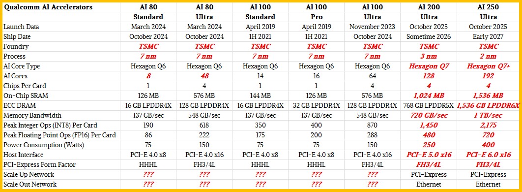
We are reasonably sure that Qualcomm is making its AI XPUs at Taiwan Semiconductor Manufacturing Co; we have guessed about the process used, and as usual, our guesses are shown in bold red italics.
We know that the AI 200 coming sometime next year, with Hussain as the anchor customer, will have 768 GB of LPDDR5 main memory and will use PCI-Express for its scale up network within a rack and Ethernet to scale out across racks. That’s about it. We know that the AI 250 kicker will come in early 2027, and that Qualcomm has committed to an annual cadence for advancements for its AI accelerators.
We made estimated of what the AI 200 Ultra and AI 250 Ultra looked like mostly to amuse ourselves, and to get a feeling for how these might look.
Not much detail is known about the architecture of the chip used in the AI 100 series. It supports FP16 floating point and INT8 integer processing and the performance the AI 100 cards along with board-level SRAM and main memory shown for the number of chips and AI cores. The AI 100 architecture is based on the Hexagon neural network processors (NNPs) that are in Qualcomm’s smartphone CPUs and that are also known as Q6 in some Linux documentation.
Here is what the Qualcomm AI core looks like:
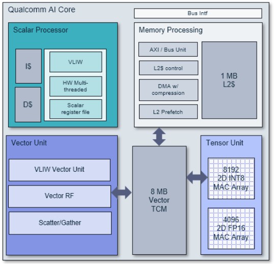
As you can see, the architecture has scalar, vector and tensor units all on the same core. It represents the seventh generation of neural network processors that Qualcomm has developed for its smartphones. The scalar chip is a four-way VLIW setup with six hardware threads; it has over 1,800 instructions. The scalar circuits have instruction and data caches and even though it doesn’t show it, there are links between the scalar unit and the memory subsystem, which is how the scalar unit offloads work to the vector and tensor units on the core. That memory subsystem has a 1 MB L2 cache that feeds into an 8 MB scratchpad memory shared by the vector and tensor units.
The tensor unit has over 125 instructions suitable for AI operations and has on 8,192 2D multiply-accumulate (MAC) array to do INT8 work and another 4,096 2D MAC array to do FP16 work. The tensor extensions are called HMX, short for Hexagon Matrix Extensions.
The vector unit has accelerators for scatter/gather collective operations and has over 700 instructions for AI, image processing, and other content manipulation functions. It can support 8-bit or 16-bit integer and 16-bit or 32-bit floating point operations. At 8-bits in integer mode, this vector unit can do 512 MAC operations per clock and at 16-bit floating point, 256 MAC operations per clock. This is obviously only a portion of the throughput of the tensor unit, but some algorithms want a vector unit, not a tensor unit. The vector instructions are known collectively as HVX, or Hexagon Vector Extensions, for short.
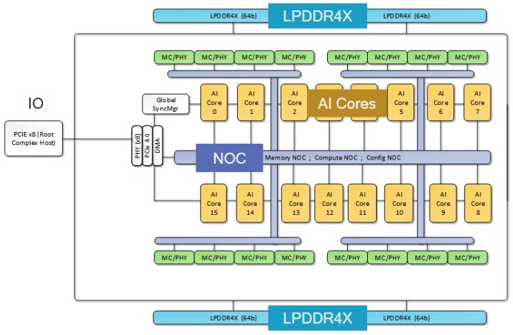
Here is what the AI 100 SoC looks like when you put sixteen of the AI cores on a die and wrap four LPDDR4X memory controllers around it plus a PCI-Express 4.0 controller with eight lanes of I/O to link to a host system:
It is reasonable to assume that Qualcomm will release a Hexagon 7 architecture with more instructions and other stuff, and also that it will boost the number of AI cores on an SoC with the AI 200 generation. To keep pace, it should be about 2X for the AI 200, etched in 5 nanometer processes perhaps to make it cheap, to get some kind of performance per watt advantage over more current Nvidia GPUs. And we think an AI 250 might boost it by another 50 percent with a shrink to 3 nanometer processes from TSMC in 2027. So 32 cores in 2026 with the AI 200 and 48 cores with the AI 250 in 2027. Clock speeds will be what they will be, based on thermals required. Expect for Qualcomm to emphasis efficiency over performance, which means lower clocks and more devices to get a given level of throughput at the same power draw as a GPU setup. This is, after all, the game that Qualcomm has been playing.
We think that the AI core also has to do at least FP8 if not FP4 precision on the tensor cores, which would double or quadruple the performance per clock cycle compared to the current AI cores based on the Hexagon 6 architecture. It is possible that Qualcomm gets rid of integer support in the tensor core and gooses floating point by a lot. (That’s what we would do.)
That brings us to CPUs. Qualcomm had an Arm server CPU called the “Amberwing” Centriq 2400, way back in 2017. It was a 48-core chip that did pretty good against the “Broadwell” and “Skylake” Xeon SPs of the time. The rumor was that Google was the backer of the Centriq effort, and for whatever reason when Google didn’t buy a lot of them, Qualcomm spiked the server CPU effort in May 2018. In January 2021, Qualcomm bought Arm server chip designer Nuvia, oddly enough not to do servers but to get its hands on its “Phoenix” cores, which are now known as Oryon cores and in contrast to the Snapdragon cores Qualcomm has designed itself.
Qualcomm has been very clear that it is once again working on a datacenter server CPU, per its May announcement with Humain. There is a good chance, we think, that the future AI 200 and AI 250 devices will have integrated server-class Oryon Arm cores integrated in the package, eliminating the need to run external X86 or Arm CPUs as hosts. And we would venture so far as to say that the LPDDR5 memory attached to the AI 200 or the LPDDR6X memory attached to the AI 250 accelerators will be shared coherently with said Oryon cores.
The statement from Qualcomm says that the AI 250 “will debut with an innovative memory architecture based on near-memory computing, providing a generational leap in efficiency and performance for AI inference workloads by delivering greater than 10X higher effective memory bandwidth and much lower power consumption.” We are not sure what that means, but it sounds like it might mean what we said above. We do not expect for Qualcomm to add HBM stacked memory to its devices, which would defeat the purpose of lowering cost and increasing availability.
That brings us to the next issue: How many Qualcomm accelerators is Humain planning to buy, and how much money is this for Qualcomm? (Which is another way of saying how much money can it take away from Nvidia.)
Qualcomm said that it has won a 200 megawatt deployment. At 250 watts for an AI 200 Ultra card with four SoCs, that is 800,000 cards. We know Qualcomm wants to deliver 160 kilowatts per rack, so say that the AI 200 Ultras are 80 percent of that power, which is 128 kilowatts. That is 512 devices per rack, and that is 1,250 racks. At $4,000 per card, that is $3.2 billion, plus maybe another $2 billion for the rack and its cooling, networking, and storage. That’s $5.2 million per rack, and if Qualcomm gets rid of integer math on the tensor cores and only does floating point and it drives the precision down to FP4 on the tensor cores, that is 983 petaflops for that $3.2 million of compute in the rack, which is $2,604 per petaflops and which is $16.30 per petaflops per kilowatt.
What does an Nvidia B300 NVL72 cost per rack, which weighs in at around 120 kilowatts to 145 kilowatts, depending on who you ask and the conditions. Not including storage, but just the scale up networking and host compute, that GB300 NVL72 rack does 1,100 petaflops at FP4 precision (really tuned for inference, not training) and costs around $4 million. That is $3,636 per petaflops and $25.08 per petaflops per kilowatt using the 145 kilowatts per rack figure. That’s about 35 percent better oomph per watt to the advantage of Qualcomm.
At $6,150 per unit for the AI 200 Ultra – if it looks like we think it might – then the performance per watt is the same between the GB300 rack and the AI 200 Ultra rack. Qualcomm can cut down from there as market conditions dictate, and maybe it will not have to discount much at all because of supply shortages and the desire to have multiple suppliers.

Dell’s AI Server Business Now Bigger Than VMware Used To Be
We have been watching the big original equipment manufactures like a hawk to see how they are generating revenues and income from GPU-accelerated system sales. These OEMs provide the best indicator of the health of the GenAI revolution and the efforts to democratize the massively parallel – and massively expensive …
Excelero Storage Deal Gives Nvidia A Nearly Complete HPC/AI Stack
In case it is not immediately obvious, over the past decade Nvidia has been transforming itself from a component supplier into a complete platform provider. Such a move was not necessary – you can expect for AMD to be pretty gun shy about such a move after is acquisition of …
There’s Still A Long Way To Go With Generative AI
The tech world is awash with generative AI, which for a company like Nvidia, is a good thing. The company that a decade ago put its money down on AI to be its growth engine has in the intervening years been pulling together the bits and pieces of hardware and …
Thank you for the interesting article. Since the Qualcomm AI250 is for AI inference and will ship in 2027, it seems unlikely to me that it will use LPDDR6X DRAM. The memory type that makes the most technical sense for storing parameters for AI inference in that time frame is High Bandwidth Flash (HBF) with a logic die for the decode phase of AI inference as the bottom die of the HBF stack. That is probably what Qualcomm meant by “near-memory computing”. The arithmetic for the decode phase of AI inference is nearer to the memory than doing that arithmetic in the ASIC. The ASIC would do the arithmetic for filling the key-value cache, called the prefill phase or prompt encoding phase. HBF will provide more bandwidth, less power consumption and less cost per GByte than LPDDR6X DRAM. If Nvidia, Apple and OpenAI buy all available capacity of HBF in 2027, Qualcomm would be better off working with Micron or some other flash manufacturer to make something similar to HBF.
The PCIe cards used in the Qualcomm AI200 sound similar to Intel’s Crescent Island. Both are PCIe inference cards that use LPDDR5X DRAM to store parameters, 160GB for Intel and 768GB for Qualcomm. Intel says sampling of Crescent Island is expected in the second half of 2026.
In the second from the last paragraph of this article, I think Timothy Prickett Morgan meant a GB300 NVL72 rack is priced at around $4 million, not $4 billion. In the third from the last paragraph, it appears that 800K cards was multiplied by $4K per card to get $3.2B of AI200 cards. That would leave no power for anything except the AI200 cards. I think what Timothy Prickett Morgan intended is to assume 80% of the 200MW deployment is for AI200 cards. That’s 160MW for AI200 cards. At 250W per AI200 card, that’s 640K AI200 cards. At $4K per AI200 card, that’s a total of $2.56B for AI200 cards. Add $2B for the compute chassis, cooling, networking, and storage for a total of $4.56B. Assume 512 AI200 cards per rack: 640K cards / 512 = 1250 racks. If the total deployment is $4.56B and there are 1250 racks: $4.56B / 1250 racks = $3.6M per rack. The picture of the Qualcomm rack in the article looks like it has 32 1U servers. It would be impressive if Qualcomm fit 512/32 = 16 liquid cooled 250W cards plus the CPUs that control the cards in a 1U chassis.
Yes, those were the assumptions I was making. 80 percent of the power for the cards.