
If you think designing a new CPU from scratch is hard, you ought to try raising money to do it. Even when there is a political and economic will to do so, as is the case with the European Processor Initiative, it has still taken longer for Silicon Pearl, the company that is creating Europe’s first indigenous CPU in a long time, to raise the money to build out its roadmap of Arm-based CPUs for high performance computing.
But, to the great relief of Philippe Notton, chief executive officer of the French startup, €90 million in Series A funding ($98.2 million in US dollars) to finish off the design of its “Rhea” processor and get it into the field next year in what we presume will be a couple of high-profile supercomputers. The money has been a long time coming, and this is not exactly the best economic environment in which to do it.
“The Series A has been much more complex to achieve,” Notton told us with his usual cheerful frankness. “We are in Europe, we are not in California. But finally, we made it, and we did this with mostly European money, which is quite important for what we are building. We are focusing on the tape out of Rhea and its use in the first European supercomputers next year. Our roadmap has been unfortunately delayed due to the complexity of raising the money.”
Let’s talk about the money, which makes the chip world go round, and then what we know about the Rhea design as it now stands, and then finish with what the roadmap might look like going forward. SiPearl was founded in 2019 and received its initial funding of €6.2 million (about $6.7 million at the time) from the European Processor Initiative, which was also formed in the summer of 2019.
The Series A financing for SiPearl includes investments by Arm Holdings, which seems obvious, as well as the Eviden systems business that is part of French IT giant Atos Group and that is being spun out into a separate company. The European Investment Council kicked in €15 million ($16.3 million, already announced), the European Investment Bank put in another €25 million ($27.2 million) in convertible debt, and the French government, under the auspices of its €54 billion France 2030 investment plan, also invested in SiPearl. We don’t know how much money the French government, Arm, and Atos individually kicked in, but if you back out the numbers we do know, then the three collectively only put in €50 million ($54.4 million). That is 1/1,000th of the France 2030 plan. It is also tiny compared to the €8 billion EuroHPC Joint Undertaking that is part of the European Horizon 2020 program. All told, including €20.5 million in grants from the EPI effort (which were paid by the EU and French governments), SiPearl has raised €110.5 million ($120.5 million).
Because Notton said the Series A was “mostly European money” and Arm Holdings is still owned by Japanese conglomerate SoftBank, you might infer that Arm, through its parent, did not kick in very much dough. We are not inferring anything. But you might.
SiPearl says that other investors are expected to join the Series A funding round before the end of the year, and it is likely that other European countries, particularly those who will benefit from Rhea and other Arm server chips from SiPearl, will invest as well. But we shall see. Considering what it takes to build a good team and design a modern CPU, all of the investors might have been more generous. (Perhaps they all had their money in Silicon Valley Bank?)
That said, SiPearl has come a long way from the ten engineers it had back in June 2020 when we did an in-depth interview with Notton about the “Rhea” and “Chronos” CPUs it was designing to meet the desires of EPI. At that time, Notton had hoped to have over 200 people working at SiPearl by the end of 2022, and as it stands, the company has only 130 as of today working in France, Germany, and Spain. But thanks to the Series A funding, and future investments it expects, the plan is to have over 1,000 employees by the end of 2025. Plenty of time before the next supercomputing cycle begins in 2028 through 2030.
And it will no doubt take plenty of dough to get the “technical sovereignty” Europe has long desired as well as the European supercomputers that “reach exascale power with back-door free security and reduced energy consumption,” as SiPearl put it in the statement accompanying the funding announcement. And we thought EPI was just about indigenous control and design and not abdicating control of compute to American CPU and GPU makers. . . .
As for a roadmap update, Notton does not yet have one, but will share one when SiPearl does.
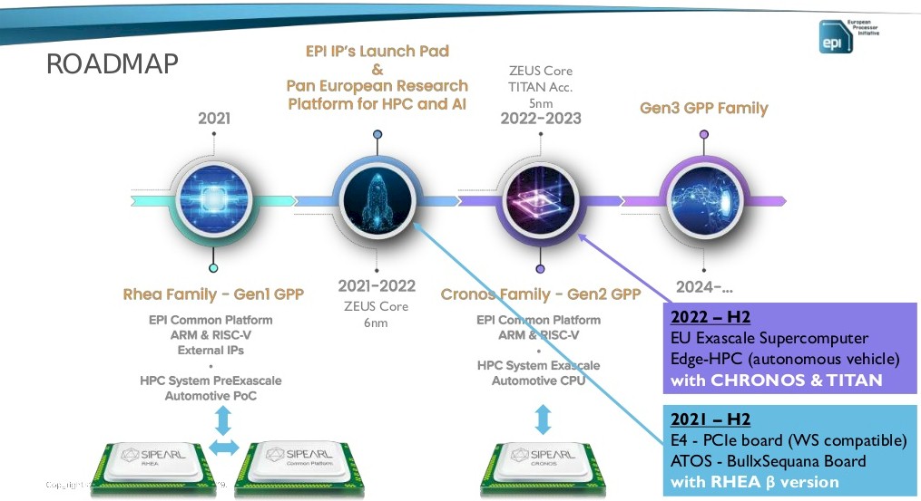
It is reasonable to assume the last roadmap we did see, from early 2020 and shown above, gets tweaked with process shrinks from foundry partner Taiwan Semiconductor Manufacturing Co. Other things no doubt have changed, too, with requirements. Notton did say that the Rhea 2 chip – which he did not call Chronos – would use more advanced TSMC processes and would come faster than the 24 month cadence that generally SiPearl wants to follow with its CPU introductions.
Back in September 2020, after our deep dive story went to press, SiPearl accidentally (or cleverly) outed the block diagram of the then-current Rhea chip design in a Tweet, the image of which we zoom in on below:
If you look carefully at that image, in the upper left, it says: “Rhea in TSMC N7 4 x HBM2E, 4-6 DDR5”
That seems simple enough, but in June 2020 Notton told us that SiPearl have shifted to the N6 process from TSMC, which is a refined variant of 7 nanometer EUV processes from that chip foundry. OK, sometimes graphics do not get updated.
Here is the other weird thing. This shows what looks like 72 cores and 36 routers linked them together and to the memory and peripheral controllers. But notice this: The mesh interconnect rails slice the cores from the L3 cache segments, and there is a grouping of 24 cores in the center of the chip that have another mesh pipe running through them. No matter how I look at this, I see some cores without L3 caches right next to them, and frankly I don’t see how this is possible. This Rhea 1 chip might only have 68 usable cores. There may be redundancy to improve yield, or this may be an error in the block diagram SiPearl had on display way back in September 2020. I can’t believe a single transistor is wasted.
The other thing to note is that back when we talked to SiPearl nearly three years ago, Arm Holdings had not yet forked its Neoverse cores and chip designs to have skinny vector (N) and fat vector (V) variations, and so do not get confused when our original story says that SiPearl was using the ‘Zeus” N2 core. That was the name of the core at the time. But in September 2020, Arm diverged its two cores, with the Zeus core being redesignated as the V1 and the N2, with a pair of SVE vector units weighing in at 128 bits wide each, being called “Perseus.” The V1 cores, which are used by Amazon Web Services in the Graviton 3 processor, have a pair of 256-bit wide SVE vector units and a tiny bit more clock speeds as well inherent in the design. The Rhea 1 chip will use the Arm V1 cores, again, still called by the Zeus code name and what N2 was originally going to be until the cloud builders and hyperscalers asked for a lower power, lower vectored core option for some of their workloads.
For Rhea 2, it is reasonable that SiPearl will use the 4N process from TSMC (a tweak on the 5 nanometer process), the one that Nvidia used to create its “Hopper” GPU and that is having its yield curve bent in the proper direction by the ramp of said Hopper GPU. By the time SiPearl needs the 4N process, it will be mature enough to have better yields than it does right now and certainly a lot better than it did last year.
Here is the official block diagram for Rhea 1 as of today:
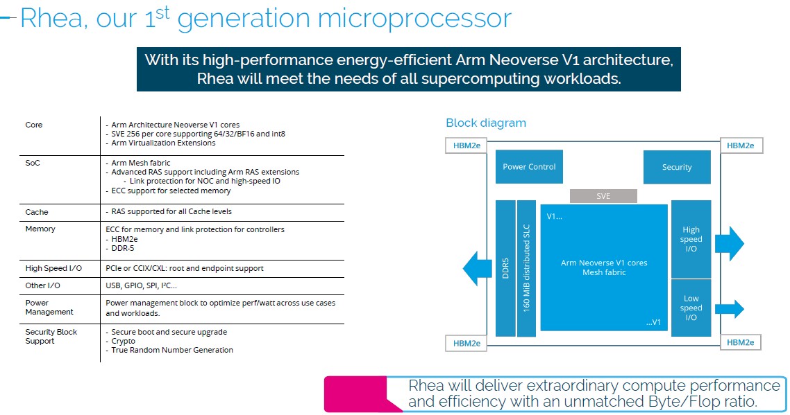
Like the “Sapphire Rapids” Xeon SP HBM variant, which is called the Max Series CPU officially by Intel, the Rhea 1 chip will allow a mix of plain vanilla DDR5 and HBM2E stacked memory. This stacked memory is a key performance enhancer for memory bound workloads – particularly certain HPC simulation and modeling workloads – as Intel has shown. We expect no different from Rhea 1.
You will also note the 160 MB of last level cache on the Rhea 1 chip. If the design has 160 MB of usable cache and there is a nice, roundish 2.5 MB of cache per core, then that is 64 cores of processing. If you can stomach 2.35 MB cache sizes, then it is 68 cores, and if we have misread the block diagram posted to Twitter in September 2020, then it is 2.22 MB of cache per core across 72 cores.
Whatever it is, we will find out and let you know.
The Rhea 1 chip will tape out later this year and start appearing in supercomputers early next year.

Debunking Datacenter Compute Myths, Part Two
Welcome to the second part of our Debunking Datacenter Compute Myths series. In the first part of this series, which you can see here, as well as in this second part, The Next Platform sat down with Lynn Comp, vice president in AMD’s server business unit, to talk about some …
Who’s Going To Build The UK’s Homegrown Exascale Supercomputer?
The years-long run-up to the first exascale supercomputers was really a story about the ongoing competition between the United States and China. Who was going to get there first? How long was it going to take? How much of an advantage would the country with the first exascale systems see …

The Impending AMD Milan Versus Intel Ice Lake Server Showdown
What a strange server CPU world we live in. The dozen or so biggest customers in the world command something on the order of 45 percent of the server CPU shipments, but significantly lower share of the revenue because of the volume discounts they can command, and they not only …
Great to see this update on the EU HPC ARM effort! If the L3 are the larger green squares, then I think each is paired with the core directly across the interconnect (white band) from it (rather than with the visually more-directly-accessible core — for some French reason). I wonder why they didn’t group the 24 top cores, and the 24 bottom cores, in the same way as the 24 central cores (with the shoelace interconnect) — if it’s good for the goose, it should be good for the “foie gras”! Yet, I think that I would suggest a quadtree organization of the cores (eg. 64 of them) and interconnect instead, to get O(log2(n)) intercore hopping, at low cost, Hanan Samet-style (former UMCP colleague) — a few of the FEA mesh generation, and broader matrix decomposition strategies covered in recent TNP articles were similarly based on quadtrees (2-D) and octrees (3-D). The pastry known as “mille-feuilles” could also, I think, inspire some tasty hyper-space connectivity (better than the accordéon) … hmmmm, yummy, … food for thought!
Agreed on the L3 and cores, but there are still four cores without L3s at the corners then.
And humorous Hu per usual.
Thanks again for the kind words! I’m looking forward to getting my mind blown clean-off by EU HPC designs, as it has been by Fugaku’s A64FX, and Frontier’s EPYC+MI250x, and will likely be as well (in June?) by GH100, SR/SP Max, and/or MI300A! If they put as much attention and creativity to this as they do to gastronomy, it should end-up in pure computational bliss!
Hot drink pointing at the hot center CPU stripe. Maybe the best cooling pipe will flow over that stripe?