
If there is one bright spot in the Xeon SP server chip line from Intel, it is the version of the “Sapphire Rapids” Xeon SP processor that has HBM memory welded to it. These chips make a strong case for adding at least some HBM memory – or something that looks and feels like it – to compute complexes that are working on HPC and AI workloads that are memory bandwidth bound and therefore cannot – and do not – squeeze every bit of performance out of the CPUs they run on.
As we previously reported, this future Sapphire Rapids HBM processor will be sold by Intel under the Max Series brand, as will the “Ponte Vecchio” GPU formerly know by the Xe HPC brand. The way Intel sees it, and speaking very generally of course, HPC and AI workloads fall into roughly three buckets. About 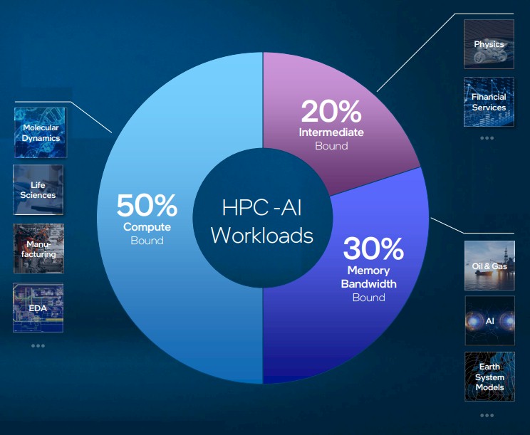 50 percent of them are compute bound, about 30 percent are memory bandwidth bound, and the remaining 20 percent are a combination of the two. Workloads that are bound by memory bandwidth include weather modeling, seismic processing and reservoir modeling in the oil and gas industry, and AI training. Compute bound workloads include molecular dynamics, protein sequencing, and anything crunching dense linear algebra equations. Risk modeling in the financial services sector is in the middle of these two extremes, and both crash simulation and computational fluid dynamics, like risk modeling, like CPU frequency over CPU throughput and are either more or less sensitive to memory bandwidth (crash simulation less so than CFD).
Addressing these distinctions across workloads means having different kinds of compute and memory in different mixes to optimize for different workloads. And that, in a nutshell, is why Intel has to have GPUs with HBM, CPUs with DRAM, and CPUs with HBM in its lineup.
The Sapphire Rapids HBM chip, which will be launched on January 10 with the rest of the fourth generation Xeon SP family, has four compute tiles, each with 14 usable “Golden Cove” P-cores, short for “performance cores” as opposed to E-cores, short for “energy efficient cores.” The Sapphire Rapids HBM compute and memory complex always has four tiles activated, with up to 56 working cores, and four HBM2e memory stacks activated, each with 16 GB of DRAM capacity for a total of 64 GB. That works out to more than 1 GB of HBM2e memory per core, and at in excess of 1 TB/sec of bandwidth per socket (we think it is around 1,230 GB/sec), that works out to around 22 GB/sec per core. This is roughly 4X the bandwidth you can expect from the plain vanilla Sapphire Rapids Xeon SPs using DDR5 main memory and eight memory controllers.
The Max Series CPU will have up to 112.5 MB of L3 cache and will support DDR5 main memory as well as that HBM2e memory, with up to 16 memory sticks per socket, one DIMM per channel, running at 4.8 GT/sec speeds and offering up to 6 TB of capacity per socket with fat DIMMs. The UltraPath Interconnect 2.0 NUMA protocol runs over the EMIB chiplet interconnect, and according to Ugonna Echeruo, chief architect and principal engineer for the Max Series CPU, presents the Sapphire Rapids compute complex as a “logically monolithic” die.
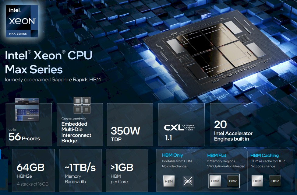
Importantly, HPC and AI shops can use a mix of standard DDR5 memory and HBM2e memory, if that suits their workloads, or they can just use HBM2e memory instead of plain vanilla DDR5 memory if their HPC and AI solvers can fit in a 64 GB memory footprint along with a little Linux kernel action. Whether the HBM memory is used alone or as a fast cache for DDR, there is no changes in the application code. There is a third mode where the HBM and DDR5 memories are presented as a single, flat address space, and there is some code optimization that will be required to optimize data placement on these two memories
Where The Memory Hits The Code
The performance gains that Intel is showing for the HBM variant of Sapphire Rapids are astounding, and if anything, demonstrates that its server CPU designs have not really been trying to run HPC and AI workloads well because they are starved for memory bandwidth. HBM memory is now established enough that it can be used on server CPUs, not just on exotic GPUs. And the fact that Intel has to gain expertise in GPU manufacturing with HBM memory means it might as well get experience and volumes with its Xeon SP CPUs by adding HBM to them. It is a fair bet, especially given the performance increases Intel is showing with its HBM server CPU variant.
Way back in February, at its Investor Day 2022 meeting, Intel was showing off this performance chart for what would ultimately be called the Max Series CPU, in this case running the OpenFOAM computational fluid dynamics application simulating the flow of air around a motorcycle with 28 million cells:
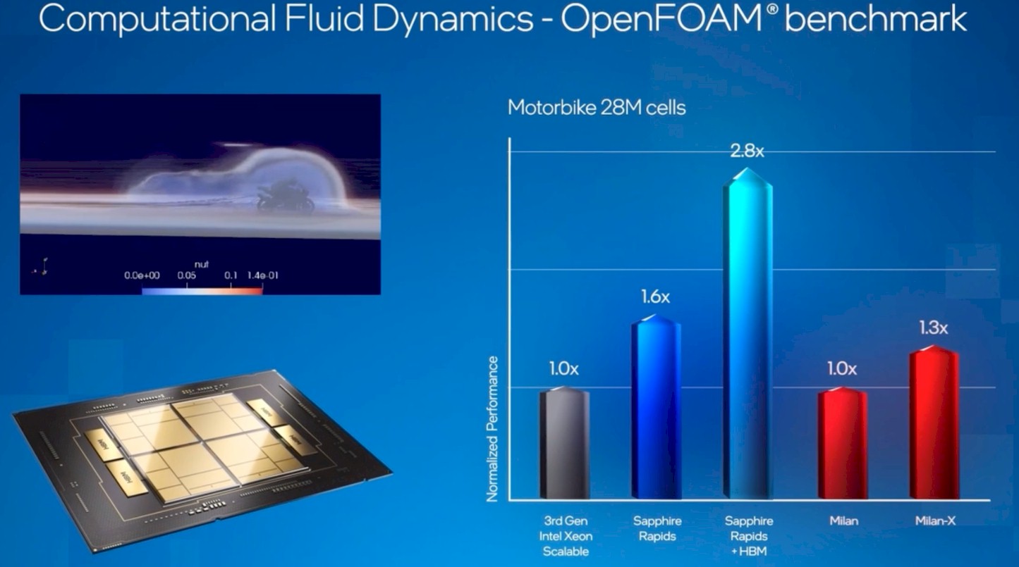
It is important to realize that the performance of the Intel Xeons and the AMD Epycs shown in the chart above are relative within their Xeon or Epyc options, but are not relative across the Xeons and Epycs shown.
Moving from a 40-core “Ice Lake” Xeon SP to a 56-core “Sapphire Rapids” Xeon SP will boost OpenFOAM performance by 60 percent – we do not know the clock speeds and the IPC deltas for the difference between the “Sunny Cove” cores used in Ice Lake and the Golden Cove cores used in Sapphire Rapids, but assume it is in the same 19 percent boost in IPC seen with the desktop CPU parts and assume there is a 40 percent increase in the cores. Then to get a 1.6X delta seen with the High Performance Linpack (HPL) test shown below, the clock speeds have to drop from 2.6 GHz on the Ice Lake Xeon SP to 2.5 GHz on the Sapphire Rapids Xeon SP.
Now, if you take that Sapphire Rapids chip and you turn on 64 GB of HBM2e memory (presumably as the only main memory on the system), then you can boost the performance on OpenFOAM by 2.8X over that baseline, top-bine Ice Lake server CPU. That is another way of saying that by using HBM memory, you can eliminate three Ice Lake CPUs from your cluster and replace it with one Sapphire Rapids CPU.
If the HBM uplift is not crazy, then for memory bandwidth bound applications, Intel should be able to sell a healthy number of Sapphire Rapids CPUs with HBM into the HPC space. (Which is why you see a large number of these CPUs yet to be delivered as part of the new “Leonardo” system at Cineca in Italy, which just entered the Top500 rankings.)
By comparison, moving from a Milan chip to a Milan-X chip with 3D V-Cache (triple the L3 cache, stacked up two high) only boosts OpenFOAM performance by 30 percent.
To which we say: We want CPUs with both 3D V-Cache and HBM. We also want direct comparisons here between the Xeon SPs and Epycs.
Intel rushed out its announcements about the Max Series CPU ahead of the AMD “Genoa” Epyc 9004 server chip launch last week, and that was so it could make more comparisons to the Milan-X 7773X chip instead of the top-bin Genoa part, which will be goosed with 3D V-Cache next year.
As far as we know, AMD has no intention of adding HBM memory to its Epycs, but based on what Intel is seeing, it very well could change its mind. AMD certainly knows how to do it, being one of the innovators of HBM memory and a GPU maker in its own right with more volumes than Intel will have for a couple of years. (And still far less volumes, in terms of datacenter compute, than what Nvidia does a year, of course.)
Here is a broader and more useful set of benchmarks that Echeruo shared. The first shows how the HBM variant of a 56-core Sapphire Rapids stacks up to an Ice Lake Xeon SP-8380 running HPL. HPL is not particularly bandwidth bound, of course, so the performance increase by moving to the Max Series CPU is only 1.4X.
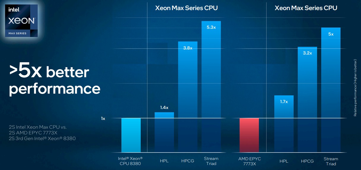
This is actually less than you would expect based on core counts and IPC, and is actually just based on core count since the AVX-512 units have not really changed all that much with the Golden Cove cores. But look at what happens on the High Performance Conjugate Gradients (HPCG) and Stream Triad benchmarks, both of which are heavily dependent on memory bandwidth. (Stream Triad is the test for memory bandwidth, in fact.) The performance increases are 3.8X and 5.3X, respectively.
And on the same tests, Intel will show 1.7X better performance on HPL compared to an AMD 7773X with 3D V-Cache, and 3.2X better performance on HPCG and 5X better performance on Stream Triad.
Here are some more general comparisons of the AMD 7773X versus the Max Series CPU on 19 different HPC and AI workloads:
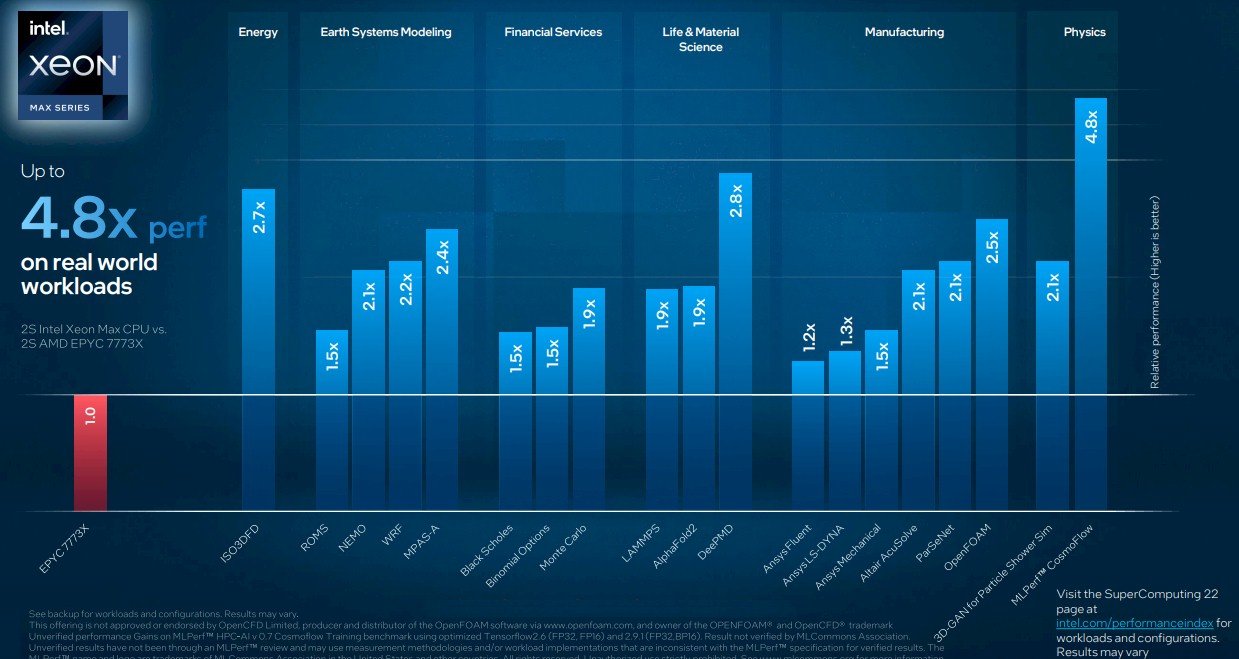
Generally speaking, the HBM variant of Sapphire Rapids is going to offer somewhere around 2X the performance of an Ice Lake Xeon SP and a Milan Epyc 7003. Now all that Intel has to do is not make it cost 2X as much and then it might actually sell some.
The math we are itching to do is how many “Skylake” and “Cascade Lake” Xeon SPs can be replaced by a Sapphire Rapids HBM socket, and how much money will that save or allow to be plowed back into more compute capacity. If Intel plays this right, it can make some happy customers and gain some goodwill as well as some desperately needed HPC and AI revenues.
The Max Series GPU Formerly Known As Ponte Vecchio
As part of the Intel prebriefings by Intel ahead of the AMD Genoa launch and the SC22 supercomputing conference, Hong Jiang chief GPU compute architect at the company provided a bit more insight on the Max Series GPU.
We have been over the Ponte Vecchio architecture at length, so we are not going to repeat all of that again. But we will tell you some incremental things that Jiang said to make more clear the competitive positioning that Intel will have with the Max Series GPU.
A quick review. The Xe core has eight vector engines and eight XMX matrix engines, plus a shared L1 cache weighing in at 512 KB. An Xe stack has 128 of the Xe cores, 128 ray tracing units for graphics, and up to eight hardware contexts (sort of like a NUMA region), plus eight HBM2e controllers and 16 Xe interconnect links. The full Ponte Vecchio device has two of these stacks, and is expected to deliver the following peak theoretical performance at various precisions:
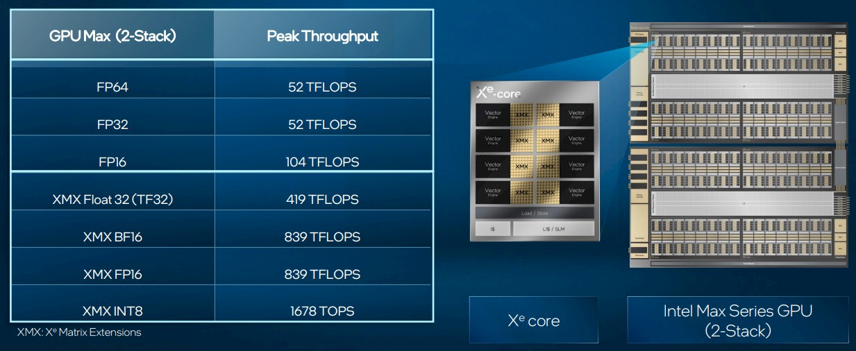
Intel has goosed the clock speeds by around 15.5 percent and is now saying it can deliver 52 teraflops at single-precision and double precision across a double stack of Xe complexes instead the 45 teraflops it was quietly (and not precisely publicly) promising a year ago. So this chart above is the stake in the ground.
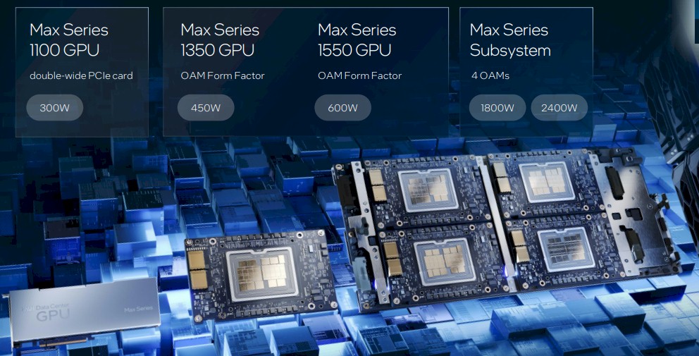
What we have learned from the briefings is that the PCI-Express versions of the Max Series GPUs only have one stack of compute, while the full-on OAM versions have the full two stacks. There is a possibility that Intel could deliver a two stack version of the PCI-Express cards, but for now, all of the OAM versions of these two stack Ponte Vecchio GPUs are going into the “Aurora” supercomputer at Argonne National Laboratory and will presumably then go into similar HPC and AI systems from Hewlett Packard Enterprise, Atos, Lenovo, and others.
By limiting the PCI-Express cards to a single stack, and therefore half of the performance, Intel can make use of the Ponte Vecchio units that are assembled but don’t fully work. As we said before, we have heard that the packaging yield on the Ponte Vecchio units is around 10 percent, so Intel has to do what it can to make money off of every part it makes.
We also got some insight into the cache hierarchy in the Max Series GPU from Jiang. The impending Intel datacenter compute GPU has two L2 caches, as shown here:
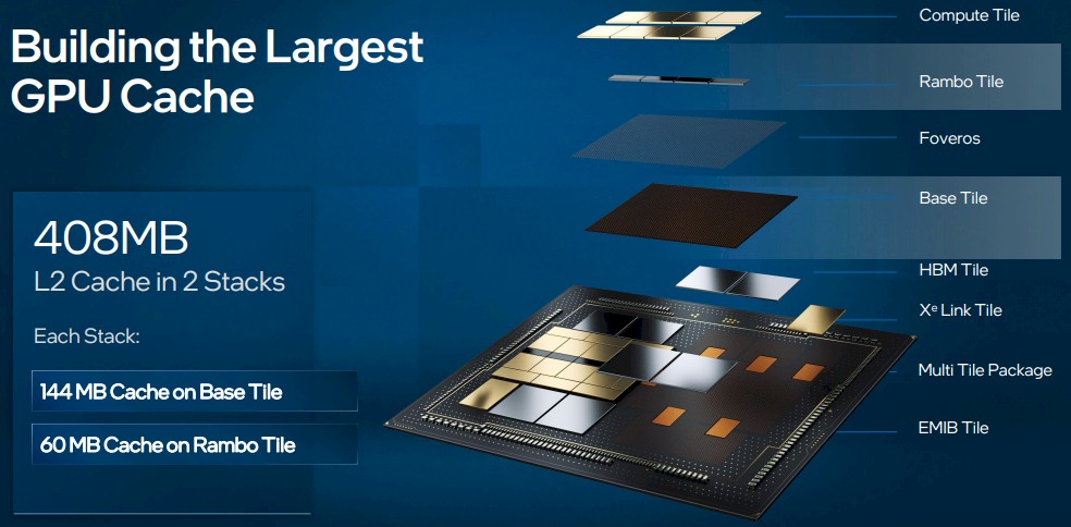
On each stack, there is 144 MB of L2 cache on the base tile and then an additional 60 MB of cache on the so-called “Rambo tile” that sits above the base tile and underneath the eight Xe compute tiles. That’s a total of 408 MB of L2 cache across the two Xe stacks.
Here is how the cache and memory capacities and bandwidths across the Ponte Vecchio device stack up:
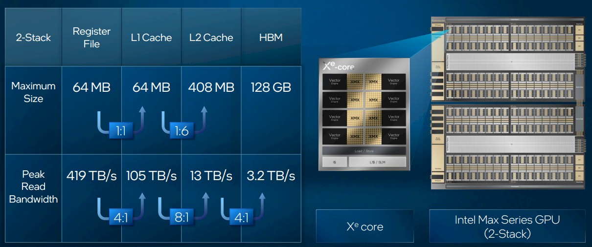
That 128 GB of capacity and 3.2 TB/sec of bandwidth across the Max Series GPU is competitive, just like that 52 teraflops of FP32 and FP64 performance is. We don’t normally see all of the bandwidth ratings for register files, L1 caches, and L2 caches for other GPUs, but these seem sufficiently large to our eye.
By the way, Jiang says that the Ponte Vecchio looks like one big GPU to software, but in a higher performance mode (this is where those eight contexts akin to NUMA regions come in) the device is configured with only two contexts – one for each Xe stack.
And then, Jiang brought it all together, showing the relative performance of the LAMMPS molecular dynamics simulator, created by Sandia National Laboratories, used in both life sciences and materials science. In this case, these are direct comparisons of two-socket Ice Lake Xeon SP-8380 and AMD Epyc 7773X servers with 256 GB of memory with a pair of Sapphire Rapids HBM sockets with 128 GB of HBM memory. And then, just for fun, Intel added performance for the two-CPU and six-GPU nodes that will be used in the “Aurora” supercomputer at Argonne National Laboratory – one with DDR5 memory on the CPUs and one with HBM memory on the CPUs. As you can see, there is a factor of 10X performance increase adding the GPUs to the HBM-boosted CPUs, and a factor of 16X better performance compared to a two-socket AMD Milan-X 7773X server.
The question is this: Will the full-blown Max Series node cost less than 16X that of a server with a pair of those Milan-X processors? It had better deliver better price/performance and better performance per watt, or there is no point other than a density increase. And that is not worth much, to be honest, all by itself.

AMD Plots Interception Course With Nvidia GPU And System Roadmaps
To a certain extent, Nvidia and AMD are not really selling GPU compute capacity as much as they are reselling just enough HBM memory capacity and bandwidth to barely balance out the HBM memory they can get their hands on, thereby justifying the ever-embiggening amount of compute their GPU complexes …
The Third Time Charm Of AMD’s Instinct GPU
The great thing about the Cambrian explosion in compute that has been forced by the end of Dennard scaling of clock frequencies and Moore’s Law lowering in the cost of transistors is not only that we are getting an increasing diversity of highly tuned compute engines and broadening SKU stacks …

With Cloud HPC Toolkit, Google Pursues HPC, Intel Pushes OneAPI
The people running Google Cloud can see the tides of HPC changing and know that, as we discussed only a few months ago, there is a fairly good chance that more HPC workloads will move to cloud builders over time as their sheer scale increasingly dictates future chip and system …
Great feeds and speeds! The HPCG results in particular, seeing how Fugaku (A64FX with HBM2) has roughly 1/3 of the performance of Frontier on HPL (EPYC+MI250x), but beats it by a tad on HPCG (16 vs 14 PFlop/s) — and here, similarly, we see Intel Max-with-HBM run HPCG 3x faster than EPYC-without-HBM, while HPL runs at about the same speed on both. As you suggest: “AMD has no intention of adding HBM […] could change its mind” — I totally agree! HBM really helps the memory access kung-fu needed by HPCG, while the dense matrix karate of HPL is already taken care of by vector/matrix units.
> Then to get a 1.6X delta seen with the High Performance Linpack (HPL) test shown below, the clock speeds have to drop from 2.6 GHz on the Ice Lake Xeon SP to 2.5 GHz on the Sapphire Rapids Xeon SP.
Well, since the benchmark benefits from HBM, it’s not so much that the clock speed has dropped but that the system-level performance of these non-HBM examples as a ceiling due to DRAM bandwidth.
Regarding cost – that will be very interesting to see as HBM parts are not cheap, and 4 of them in the processor package will have a significant effect on the CPU cost – quite likely the 2x mentioned in the article?
But then analyzing this at the system level, the in-package HBM makes it unnecessary to have 8 memory channels per socket that are populated with server-grade memory. That’s a significant saving, and on top of that there is a board area and complexity saving, and likely also a power and cooling saving (no need to drive “long” on-board wires with their terminating resistors).
And as board area is saved, compute density goes up – so there could be some kind of virtuous spiral that comes into effect, as long as all of the active data can fit in HBM.
Totally agree. 100 MHz is a rounding error. Which was the point I was trying to make. Hey, it was late at night when I wrote this… HA!
Except I don’t know how many customers are going to skip ddr5. I think most will chose to buy both HBM and DDR5. You can make a handful of applications super fast, but there are a ton of applications that require more memory per rank. If you want to make your machine work for all the applications you have to do both. I suppose you might see a large mostly-ddr machine with a small partition of HBM nodes, much like most HPC machines have a small GPU partition. It’s really hard to buy a machine that works well for all applications, and expensive to make every node the best of the best.
the phoronix site had a couple of articles on SPR’s new user interrupt feature, bypassing kernel for interrupting other cores. They claim “9x faster for lower IPC communication latency”. Were there any comments at sc22 on what this feature contributes to hpc/ai performance?