

Historically Intel put all its cumulative chip knowledge to work advancing Moore’s Law and applying those learnings to its future CPUs. Today, some of those advanced processors are destined for the forthcoming “Aurora” supercomputer at Argonne National Laboratory. However, demanding simulation and modeling workloads also benefit significantly from GPU acceleration. Recognizing this ever-growing need, Intel set out to design and build its most complex GPU to date and do it within a very tight timeframe.
The result of this effort, Intel Max Series GPU formerly known by the code name “Ponte Vecchio,” packs 100 billion transistors and 47 tiles onto five process nodes. Beyond that, they include two packaging innovations, EMIB 2.5D and Foveros 3D technology, and stack tiles atop one another for greater processor density. “The Intel Max Series GPU development cycle was quite compressed, so bringing it to life was like challenging our team to build a house one year, then a skyscraper the next year,” said Duke Tallam, Intel Max Series GPU product manager. “To date, the GPU is our most complex processor and represents a huge leap forward among Intel’s silicon offerings. Yet, the entire package can fit in the palm of a person’s hand.”
Many Innovations Brought The Max Series GPU To Market
The immense complexity of the Max Series GPU required support from Intel team members around the globe. After completing the technology development process at factories in Oregon and Arizona, the silicon traveled to Intel’s manufacturing facility in Penang for high-volume production.
Getting to that stage, though, required creative solutions since Intel needed several modifications to its fabrication process. First, Intel shrank pitch chip wafer interconnects to 36μm, about the width of a human hair. It’s the finest-grain pitch ever used successfully in an Intel fab or factory. Intel factories also developed a novel way to test die on the factory line – called Singulated Stacked Die Test (SSDT). SSDT ensures only functioning dies move forward in the manufacturing process before adding other costly components like substrates and High Bandwidth Memory (HBM) die. The company also found a new way to solder die onto the package, boosting process capability by 50 percent. Lastly, the group developed an advanced wafer-level assembly process to improve reliability tenfold.
Beyond the GPU’s technical complexity, the validation process involved the challenge of completing pre-silicon tests on a minimal number of sample GPUs. So, instead of relying on physical samples for testing, the team turned to virtual simulations demonstrating how virtual die would perform in real-world scenarios. Elsewhere, engineers employed other creative ways to accelerate the testing process, like methodology to run parallel workstreams among the many team members working on the project.
When asked about the Herculean effort required to catapult a GPU to market in two years, Intel’s Tallam offered his perspective. “We have more than a half-century of experience making processors but designing something of the GPU’s complexity and performance requirements required all our past knowledge and skill.” Tallam continued, “The Max Series GPU helps bridge the gap between today’s already-incredible HPC systems and those few systems in the world that can or will achieve exascale-level performance. So, it seemed only right we’d name the GPU after the famous bridge in Florence, Italy. The Max Series GPU bridge is both beautiful and extraordinarily capable. Our team feels the same way about the GPU at a much tinier scale.”
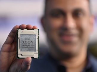
The combined power of these datacenter GPUs with the newly introduced Intel Xeon CPU Max Series processors will accelerate workloads to reveal valuable results in a much shorter time than possible previously. The Argonne National Laboratory is among the first Max Series adopters. Its team plans to deploy 60,000 of Max Series GPUs divided equally among 10,000 server blades. Each blade will also rely on two Intel Xeon CPU Max Series processors (these are the “Sapphire Rapids” Xeons SPs with HBM memory) to maximize Aurora’s architecture for some of the most significant scientific workloads ever undertaken. Once ANL deploys a full complement of the Max Series GPUs and CPUs on their flagship Aurora system, it will exceed two exaFLOPS of double precision compute performance.
Researchers already plan to use all that computing power on some of the most challenging scientific problems like modeling the universe, advancing safe fusion-based energy solutions, helping with medical breakthroughs, or forecasting hurricanes with higher precision.
These GPUs represents a core component of Intel’s ambitious, multi-year IDM 2.0 strategy for product leadership, innovation, and long-term customer value.
Bringing It All Together
Last November, Penang Assembly and Test (PGAT) employees in Malaysia celebrated the manufacture of the first 60,000 GPUs. Malaysia hosts Intel’s largest assembly and test manufacturing facility combining four factories.

Wong Mei Fong, factory manager, Penang Assembly and Test (PGAT), has seen plenty of challenges in her 28-year Intel career. Still, they all paled in comparison with the GPU’s complexity and coordination across 1,500 team members. PGAT needed to meet production demand in half the time typically associated with a project of this magnitude. To make it all possible, other teams and factories also supported the effort.
“The numerous complexities of this product are unrivaled. The steep challenge we faced was made even more difficult with our compressed timeline,” said Mei Fong. “Despite these obstacles, we achieved what seemed impossible initially with invaluable help from our partner organizations.”
Valuable Lessons
The combined learnings from developing and manufacturing the GPU Max Series bring new insights for future production processes that will accelerate the delivery of forthcoming processors. Tallum noted, “We’re excited about our latest processor releases, and we’re proud to have an opportunity to do our part to enable breakthrough science.”
Rob Johnson spent much of his professional career consulting for a Fortune 25 technology company. Currently, Rob owns Fine Tuning, LLC, a strategic marketing and communications consulting company based in Portland, Oregon. As a technology, audio, and gadget enthusiast his entire life, Rob also writes for TONEAudio Magazine, reviewing high-end home audio equipment.

Deep Dive Into Intel’s “Ice Lake” Xeon SP Architecture
No question about it. Intel had to get a lot of moving pieces all meshing well to deliver the “Ice Lake” Xeon SP server processors, which came out earlier this month and which have actually been shipping to a few dozen select customers since the end of 2020. Getting the …
HPC In 2020: Compute Engine Diversity Gets Real
The choice of processors available for high performance computing has been on growing for a number of years. There are no less than three major types of CPUs available for HPC duty, including X86, Arm, and Power architectures with more than a half dozen credible suppliers in total, along with …

AI At The Edge Is Different From AI In The Datacenter
Today’s pace of business requires companies to find faster ways to serve customers, gather actionable insights, increase operational efficiency, and reduce costs. Edge-to-cloud solutions running AI workloads at the edge help address this demand. Placing compute power at the network edge, close to the data creation point, makes a vital …
Out of curiosity, how many pins does the GPU chip have?
More than a grenade, less than a spinster.
The most complex chip ever made, better say: the delay chip ever made, Aurora HPC wait, wait, and wait…many years