

Moore’s Law is not just a simple rule of thumb about transistor counts, it’s an economic, technical, and developmental force—and one strong enough to push some of the largest chipmakers to future-proof architectural approaches.
That force pushed some of AMD’s lead architects to reroute around the once-expected cadence of new technology development by pursuing a chiplet approach. We’ll get more to the reasons why and what they considered in a moment but first, it’s useful to lay the groundwork.
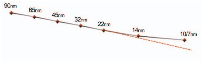 AMD revealed its own internal estimates (right) for rough dates important new process nodes emerged over the last decade-plus. Notice what happens at 14nm—new technologies were humming along at a regular two-year clip but with that jump, it moves to three and keeps extending. That chart speaks volumes about what we already know full well. Moore’s Law is slipping and soon, that decline will be precipitous.
“The cost to manufacture an integrated chip has been steadily climbing, with a sharp increase in the latest generations due to increased mask layers (e.g. for multiple patterning), more challenging and complex manufacturing (advanced metallurgy, new materials) and more,” the AMD team explains. “Not only are processor manufacturers waiting longer for each new process node, but they must also pay more when the technology becomes available.”
The cost pressures are clear: aiming for higher densities will slow innovation at this point and, as the AMD team notes, even though the end price of high-density devices can offset some of the high costs, “the industry is now running up against the lithographic reticle limit, which is a practical ceiling on how large silicon die can be manufactured.”
“Each chiplet is manufactured using the same standard lithographic procedures as in the monolithic case to produce to a larger number of smaller chiplets. The individual chiplets then undergo KGD testing. Now, for the same fault distribution as in the monolithic case, each potential defect results in discarding only approximately one-fourth of the amount of silicon. The chiplets can be individually tested and then reassembled and packaged into the complete final SoCs. The overall result is that each wafer can yield a significantly larger number of functional SoCs.”
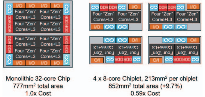
The above schematic shows a hypothetical monolithic 32-core processor. AMD says their own internal analysis and product planning exercises showed such a processor would have required 777mm2 of die area in a 14nm process. “While still within the reticle limit and therefore technically manufacturable, such a large chip would have been very costly and put the product in a potentially uncompetitive position.”
Readers of The Next Platform are already well aware of these trends, but it’s worth emphasizing because these pressures were central to AMD’s broad chiplet strategy. And this is all despite the costs of this approach. After all, if chiplets were a clear winner the entire industry would have chased it long ago.
“A chiplet design requires more engineering work upfront to partition the SoC into the right number and kinds of chiplets. There are a combinatorial number of possibilities, but not all may satisfy cost constraints, performance requirements, ease of IP and silicon reuse and more,” the AMD team explains. It also takes major R&D on the interconnect, involving longer routes with potentially higher impedances, lower available bandwidth, higher power consumption and/or higher latency. The interconnect complexity gets even farther into the weeds, with voltage, timing, protocol, SerDes changes, and being able to replicate all the testing and debugging across far more elements—all of which make chiplets look less of an apparent obvious choice.
Much of the advantage of the chiplet approach, despite those complexities, became apparent in the first-generation AMD EPYC processor, which was based on four replicated chiplets. Each of these had 8 “Zen” CPU cores with 2 DDR4 memory channels and 32 PCIe lanes to meet performance goals. AMD had to work in some extra room for the Infinity Fabric interconnect across the four chiplets. The design team talks about the cost lessons learned from that first run:
“Each chiplet had a die area of 213mm2 in a 14nm process, for a total aggregate die area of 4213mm2 = 852mm2 . This represents a ~10% die area overhead compared to the hypothetical monolithic 32- core chip. Based on AMD-internal yield modeling using historical defect density data for a mature process technology, we estimated that the final cost of the quad-chiplet design is only approximately 0.59 of the monolithic approach despite consuming approximately 10% more total silicon.”
In addition to lower costs, they were also able to reuse that same approach across products, including using them to build a 16-core part that doubled DDR4 channels and gave 128 PCIe lanes.
But none of this was free. There was latency introduced when the chiplets talked over the Infinity Fabric and given a mismatch of the numbers of DDR4 memory channels on the same chiplets, some memory requests had to be handled carefully.
These lessons were put to use with the second-generation 7nm Epyc processor. There is an incredibly rich discussion about the various tradeoffs and technical challenges as well as cost and performance found here, including factors behind packaging decisions, co-design challenges, optimizations, and cross-product expansion of a similar approach.
“In addition to the technical challenges, implementing such a widespread chiplet approach across so many market segments requires an incredible amount of partnership and trust across technology teams, business units, and our external partners,” the team concludes.
“The product roadmaps across markets must be carefully coordinated and mutually scheduled to ensure that the right silicon is available at the right time for the launch of each product. Unexpected challenges and obstacles can arise, and world-class and highly passionate AMD engineering teams across the globe have risen to each occasion. The success of the AMD chiplet approach is as much a feat of engineering as it is a testament to the power of teams with diverse skills and expertise working together toward a shared set of goals and a common vision.”

Intel Rounds Out “Granite Rapids” Xeon 6 With A Slew Of Chips
It is no secret that chip maker Intel is having a tough time these days on a number of fronts, but it is important to remember that nearly two out of every three processors sold into the datacenter are Intel Inside. This is a good business that can be moderately …
The Battle For Enterprise Compute Begins In The Cloud
If the hyperscalers are a crystal ball in which we see the far-off future of compute, storage, and networking writ large and ahead of the mainstream, then the public cloud builders are a mirror in which we see the more immediate needs and desires of enterprises. Even within those organizations …
AMD Breaks $1 Billion In Datacenter GPU Sales In Q2
As expected, AMD has once again raised its forecast for sales of its Instinct MI300 series GPUs, and as it has broken through $1 billion in revenues for its “Antares” line of compute engines in the second quarter, it is now expecting to surpass $4.5 billion in sales of these …
The return of multi-chip modules!
What I thought is particularly impressive that they have been essentially able to generate their entire second generation EPYC line-up, as well as most (all?) of their 3rd generation Ryzen line-up with just 3 chiplets — CCD, IOD, cIOD (cf Figure 23 in the paper). As the authors state, “Chiplet-based design has transformed architecture at AMD”. Great job by the AMD team!
Wish they had talked a bit about their 3D cache design too, but perhaps that’s another paper.
Wasn’t first through third generation(Zen2) four cores per CCX, two CCX per CCD, and then for Epyc, the “up to 4 CCD per chip”? The move to Zen3 eliminated the CCX/CCD and made it so each CCD is either 6 or 8 cores(where two are disabled due to faulty silicon).
Yeah, the 3D cache approach seems like it has a huge impact on chiplet strategy. It seems to have the potential to largely mitigate the latency/bandwidth/power issues associated with longer interconnects. If production can scale to meet demand, that would be a game-changer, as the future quickly becomes a chiplet dominated place.
What a wonderfully thought provoking reminder of ~Zen/Fabric’s origins.
In some ways, it was a no brainer for amd’s precarious situation (it their ~only chance of competing), but it is healthy to be reminded what a brave call it was to accept obvious downsides in favour of less obvious upsides of their design.
I hope you do another Nicole, predating the release of Epyc.
I flatter myself that i can see the seeds of the architecture in the ~2014 Kaveri AM2+ APUs, & I suspect it was tied to the logic of betting the company to buy ATI GPUs back in 2005 – ie, if they had a better integrated gpu on desktops, customers would forgive a lesser cpu, but it would be a modular cpu they could cluster and repurpose for a wide variety of markets & with attractive yields
Nvidia seems to be content with monolithic designs for now, so it will be interesting to see how the chiplet idea extends to GPUs. Seems interesting on paper anyway, so Frontier will be telling.