
Whenever a process shrink is available to chip designers, there are several different levers they can pull to make a more powerful compute engine. With the latest “Aurora” Vector Engine accelerators from NEC, long-time supercomputer maker NEC is pulling on a bunch of levers at the same time – and apparently to varying degrees to keep the chips from getting too hot.
We say apparently there because NEC’s announcement was pretty thin on the details. We have reached out with some specific questions about the new VE30, the third generation of Vector Engine accelerators to come out of NEC in the past five years and the latest in a long, long line of vector machines that stretches back as far as we can remember. But thus far, NEC has not responded.
In the meantime, as has happened before with Vector Engine announcements, we will tell you what we know and infer a little to try to fill in some gaps.
First, let’s take a look at the NEC Aurora accelerator roadmap:
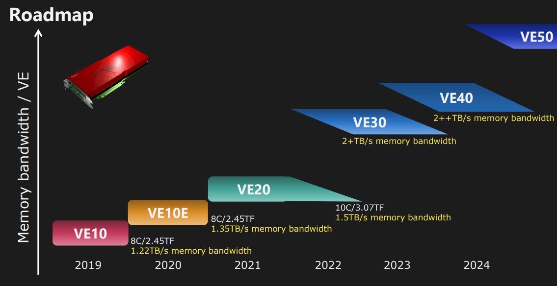
There are actually several iterations within each VE family, and all of them are based on HBM2 memory thus far. Generally speaking, NEC has been focused on growing the memory bandwidth with each generation and scaling out the compute capacity as it can. With the VE30 generation, expected about now in 2022, the roadmap promise was to deliver more than 2 TB/sec of memory bandwidth on each device, which is up there with the latest GPU accelerators on the market used for HPC and AI workloads. To be specific, the NEC roadmap called for the VE30 to have a “new architecture, larger memory bandwidth, higher core count, higher frequency, and new functions.”
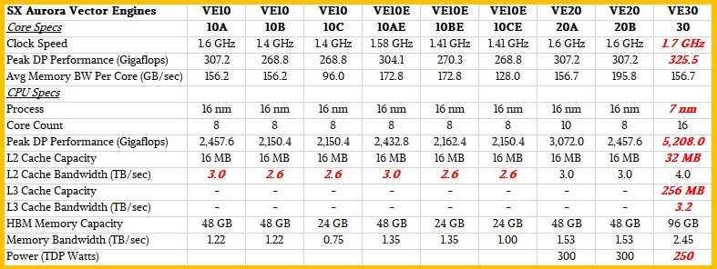
Here is what we know. The number of cores in the VE30 is 16, compared to the 10 cores in the VE20, and the memory bandwidth has increased by 1.6X and the memory capacity has increased by 2X. If you do the math on all of that, then the 16 core VE30 vector math accelerator has 96 GB of HBM2e memory (we presume NEC has not made an aggressive move to HBM3 like Nvidia has and is saving that for the VE40 upgrade coming next year) and has 2.45 GB/sec of aggregate bandwidth coming out of that HBM2e memory.
While NEC did not specify any of this, we think it has shifted from a 16 nanometer process from Taiwan Semiconductor Manufacturing Co used with the VE10 and VE20 accelerators in the Aurora family to a reasonably mature 7 nanometer process from TSMC. There is no way that NEC would have opted for the 10 nanometer shrink from TSMC – that node was not really used in high performance devices and was a tough one as it has been for Intel and GlobalFoundries. And we do not think that NEC would jump to a 5 nanometer process and there is no way it would be on the front end with a 3 nanometer process. These processes are too expensive to use for such relatively low volume products in a market with a very limited size. (Nvidia can push the envelope because it has thousands of HPC and AI customers using its datacenter GPU compute engines.)
The other bit of data we know is that Tohoku University in Japan, which has been using NEC SX series vector supercomputers since the SX-1 and SX-2 were announced way back in 1983, is going to take delivery of a supercomputer stuffed with 4,032 of these VE30 engines that is expected to be rated at around 21 petaflops of peak aggregate floating point compute at 64-bit precision. This will make the machine at Tohoku University the most powerful vector supercomputer in the world, and throughout all of computing history, and it will be 586X more powerful than the 35.86 teraflops Earth Simulator that NEC built for JAMSTEC lab in Japan in 2001.
If you do the math backwards on that, then a 16-core VE30 vector accelerator is rated at 5,208 gigaflops, and that means the peak FP64 performance per core on the VE30 is 325.5 gigaflops. That’s a tiny bit less than a 6 percent increase in per-core performance compared to the core in a VE20 vector accelerator. Which means the clock speed on the VE30 is only that 6 percent higher than the 1.6 GHz of the VE20.
This relatively low clock speed, if we have inferred correctly, is a bit surprising at first, but not if you consider that most HPC centers are as concerned with performance per watt as they are performance because electricity is not cheap.
The move from TSMC’s 16 nanometer process to its 7 nanometer process – what it calls a full node hop – delivered somewhere between 35 percent to 40 percent faster clock speeds on the transistors in the same power envelope or 65 percent lower power consumption at the same clock speed, and a factor of 3.3X higher transistor density. Rather than crank the clocks all the way up and make a huge 16-core package that runs at 600 watts or even 700 watts, NEC seems to have modestly cranked the clock speed with the VE30, doubled up the cores (possibly with a multi-chip module approach that would be a simpler design and would allow for the doubling of the memory capacity while increasing the memory bandwidth by 1.6X – and actually reduce the overall power consumption.
Here is out best guess on how the VE30 vector accelerator compares to its predecessors in the Aurora line:
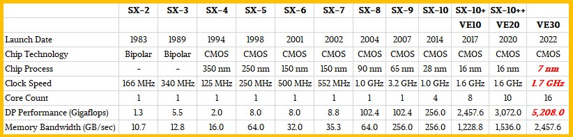
And here is how this VE30 generation compares all the way back to the SX-2 engines made by NEC:
NEC said that it has added an L3 cache to the VE30 architecture, which we presume is a shared cache for all of the cores as is done with CPUs and GPUs these days. No details were given on this L3 cache, but if the cache looks like that on modern CPUs and GPUs, it should be a factor of 4X to 8X larger than the L2 cache and it should have less aggregate bandwidth than the L2 cache but more aggregate bandwidth than the HBM2e memory. We took a stab at it and think the L3 has 256 MB of capacity and has 3.2 TB/sec of aggregate bandwidth. (We admit this is a wild guess.) The important thing is that the accelerator has 2.45 GB/sec of HBM2e bandwidth that can inject data like crazy into this L3 cache, which helps better balance out the data moving into the L2 cache. (We presume.)
Frankly, we are surprised that there is an L3 cache and NEC said this is the first time in its vector architecture that it has used an L3 cache. CPUs have a fat L3 cache because DDR DRAM is too damned slow compared to L2 cache. But this is not the case with the L2 cache compared to HBM2 and HBM2e memory, so this is a puzzling choice.
We don’t have a lot of CPUs with HBM, HBM2, and HBM2e memory to draw from as examples. Fujitsu’s Sparc64-XIfx processor used in its supercomputers many years after the launch of the “K” supercomputer had eight HBM blocks 2.2 TB/sec of L2 cache bandwidth directly linked to eight HBM1 banks with 480 GB/sec of bandwidth. The A64FX processor from Fujitsu used in the “Fugaku” supercomputer had 3.6 TB/sec of L2 cache bandwidth being fed by 1 TB/sec of HBM2 memory comprised of four blocks running at 256 GB/sec.
Nvidia, AMD, and Intel discrete GPUs have L2 cache memory and various HBM memory, but no L3 cache memory.
Presumably, Intel will ship L3 cache on the HBM version of its “Sapphire Rapids” Xeon SP processor, now expected early next year if the rumors are right. But for all we know, the L3 cache will be disabled and L2 will be linked directly to HBM memory in some fashion.
Like we said, it is a strange choice to add L3 cache to the VE30 compute engine, and we look forward to learning more.
A few more things. The rumor going around last year was that the VE30 engines would not just support FP64 double precision and FP32 single precision math, but also FP16 half precision math. The latter would make the Aurora motors suitable for running machine learning training workloads, which might be useful in expanding the market for these chips. Also, we presume that the VE30 accelerator engine comes with a PCI-Express 4.0 x16 slot on it, not the PCI-Express 3.0 x16 slot the prior generations used. And the VE40 next year should probably have a PCI-Express 5.0 slot and support for the CXL 2.0 protocol as well. Why not?

Intel Let The Chips Fall Where They Might
This day always comes. It is the nature of monopoly and hubris. It came for IBM. It came for Microsoft, and it is coming for Facebook. It will come for Google and, even though it is hard to believe, it will come for Amazon. And it is most assuredly coming …

Prime Contracting No Longer One Of Intel’s HPC Aspirations
Intel has spent the past nine months reorganizing itself in the wake of Pat Gelsinger becoming its chief executive officer in January, including new groups and divisions and new managers for them that were revealed in June. But the fate of its HPC organization, which has been less focused than …

Argonne Aurora A21: All’s Well That Ends Better
When it comes to a lot of high performance computing systems we have seen over the decades, we are fond of saying that the hardware is the easy part. This is not universally true, and it certainly has not been true for the “Aurora” supercomputer at Argonne National Laboratory, the …
My suspicion is that the L3 cache is there to support improved performance for malformed transfers to the memory. 8 stacks of HBM2 is really just like 64 channels of dram, a lot like vector processors of old, with 128bit atoms. Some memory access patterns are going to be very antagonistic to this memory layout (read every 64th word). A highly associative sram cache could greatly improve memory performance for these sorts of transfers, even with no improvement in maximum bandwidth. One wonders what the cache line size is for the L2 and the L3, and the associativity. This is really the way that NEC gets to set this thing apart. If your application is absurdly parallel, and has simple memory access patterns, there’s no way they can compete with GPUs for raw compute performance. They have to get their wins in the codes where Nvidia and AMD provide a small fraction of peak.
Glad to have you around, Paul, to take the ball a few more yards. Thanks.
If the numbers pan out, this could provide a nice uprade to Earth Simulator’s VE20 architecture (#51 in 06/22 top500), bringing it to a more interesting 40 or 50 MJ/Exaflop (vs 100 currently).