
The Hot Chips 34 conference that is normally held at Stanford University is in full swing this week, and thanks to the coronavirus pandemic is being held entirely online. Which means we have to buy our own ice cream and make our own lunches as we ponder the presentations offered up by chip vendors and academia, showing off the innovations them are bringing to bear.
The Computer Express Link, or CXL, protocol for cache and memory coherence is a big area of research and development these days, and Hot Chips hosted a tutorial on what it is, how it is evolving, and what impact it will be having on system architecture. We are well aware that alternatives such as Gen-Z (Hewlett Packard Enterprise and Dell), CCIX (Xilinx, AMD, and the Arm collective), OpenCAPI (IBM), Infinity Fabric (AMD), and NVLink (Nvidia) all have their benefits, and are each in their own ways better than the initial CXL that Intel proposed as a means of providing asymmetrical cache coherence for accelerators over the PCI-Express bus and over PCI-Express switch fabrics.
We were a little disappointed that Meta Platforms, the parent company of Facebook, didn’t say more about its plans for CXL in the tutorial. Meta went over some of work it has done with its Transparent Page Placement (TPP) that it is upstreaming into the Linux kernel, which we already covered back in June. TPP pages data into and out of both DRAM main memory attached to CPUs and CXL main memory attached through PCI-Express as it gets hotter and colder – all without having to rewrite application code. It is important, and will help hide some of the latencies that will always exist as memory, no matter how it is built, moves further from a compute engine.
We think that TPP will be an important aspect of a future memory hypervisor, which we have long thought needs to be developed independent of the server virtualization hypervisor or a container platform. We need a software memory controller to not only partition and share memory, but to glom it together across multiple (and sometimes incompatible) compute engines in a coherent fashion when appropriate and to also control the movement of data across different sockets, NUMA regions inside and outside of server node, and other higher level memory pools with differing feeds, speeds, costs, and latencies to those compute engines.
When Intel pulled the plug on Optane memory a few weeks ago, several months after former memory partner Micron Technology did so, we quipped that wherever we saw persistent memory like Optane 3D XPoint memory in system memory hierarchy, it would simply be replaced with shared CXL memory. Instead of having a cheaper and fatter kind of persistent DRAM based on 3D XPoint ReRAM to drive the price/performance of the overall system and cluster memory down and the performance up, we would have to start pooling DRAM and sharing it to drive up its utilization and thereby make better use of the expensive resources we were already paying for. 3D XPoint was more expensive than planned and slower than planned, and had the added disadvantage that Intel kept it only for its own Xeon SP processors, which have been constantly late and therefore have been stalling the Optane roadmap, too.
All’s well that ends better. The memory hierarchy is going to be smashed open, with new layers of pooled and switched memory. What Prakash Chauhan, a hardware engineer who worked at converged infrastructure pioneer Egenera back in the 2000s and has been a server architect at Google and Meta Platforms since then, called “Tiers of Happiness.” This chart was taken from the TPP paper, and it is interesting that the latencies were scrubbed from the left side of the diagram:
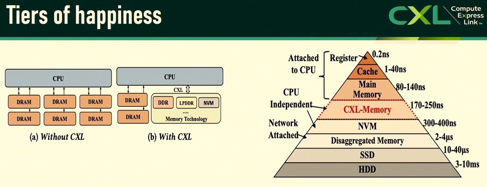
Probably because the simulations and tests that Meta Platforms ran are not representative of where CXL memory will be with future generations of the PCI-Express transport, and maybe not even with PCI-Express 5.0 and CXL 2.0.
Adding CXL memory to the storage hierarchy is not as simple as getting a shoehorn and a soldering iron and that’s that. But in two charts, Chauhan showed what the real problem that system architects are facing, and to a certain extent what Intel and Micron were hopeful they could partially solve with Optane memory when they revealed the 3D XPoint effort way back in the summer of 2015. And by the way, as our compatriot at The Register, Liam Proven, correctly pointed out in an obituary for Optane, we still need persistent main memory in systems and we still don’t have it.
In two charts, Chauhan summed up the problem with system memory these days. And added a whole loot of engineering challenges that need to be solved to get around them.
The first is that memory costs have flatlined since 2013 and are not on a Moore’s Law curve any more. Take a look:
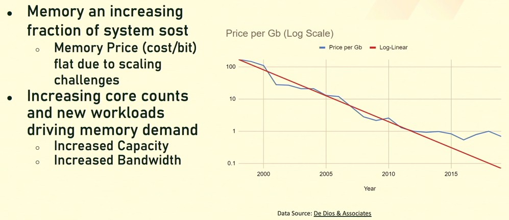
Memory vendors are building faster memory, to be sure, and denser memory sometimes, but they are not building cheaper memory. And because of this, memory represents somewhere between 25 percent and 50 percent of the cost of a system, depending on what it is doing and depending on who you ask. But it is a far cry from 15 percent. The cost of compute, storage, and networking is still coming down, and that is making memory seem even more expensive.
Even if memory was cheaper, adding DRAM controllers to any compute engine has headaches.
“Current systems require adding more DDR channels to the CPU, or moving to faster data transfer rates,” Chauhan explained in his talk. “However, because DDR is single ended, each channel added adds a couple hundred pins when we account for signals and power. This leads to expensive sockets and reduced reliability as good contact is needed to be maintained over many thousands of pins. We also need to add additional PCB layers to route these additional channels of memory, which increases PCB costs. Higher data rates also come at a cost. In order to maintain a reliable interface, we need to have better signal integrity, which means we need to minimize reflections and crosstalk – and crosstalk becomes really important for these wide parallel busses. To achieve high signal fidelity, we need to reduce pad capacitance, which can lead to expensive manufacturing processes to remove the effects of inter-symbol interference and reflections. Signal processing elements such as DFEs [decision feedback equalizers] are needed, which increases power and circuit cost. As data rates continue to ramp up, we might have to live with one DIMM per channel, which causes further problems with scaling the DRAM capacity.”
IBM has already moved to differential DIMM memory (using Bluelink SerDes as memory ports out to buffered memory cards) and one DIMM per channel with the “Cirrus” Power10 processors used in its latest Power Systems iron. (And given that IBM has donated OpenCAPI technology to the CXL Consortium just as the CXL 3.0 spec was unveiled, you can expect to see something similar in the long run with DRAM over PCI-Express.)
Aside from all of those engineering challenges with main memory, driving up memory utilization – getting the most out of the memory you do end up buying – is tough because you have to plan for peaks. And sometimes, even when you do that, you can get the ratio of compute to memory that you want. Here is a simple example that Chauhan showed:
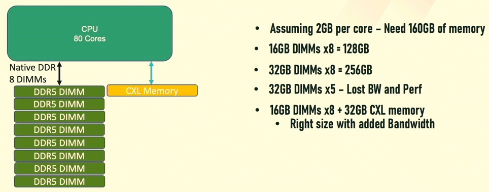
In the example above, you have a CPU with 80 cores and eight memory channels, and you want to do the classic 2 GB per core of memory capacity with DDR5 memory sticks. If you use 16 GB DIMMs, which are relatively cheap, you end up with only 128 GB. If you use fatter 32 GB sticks, then you end up with 256 GB, which is 60 percent more memory than you need so that extra money spent goes up the chimney and there is a good possibility that the memory doesn’t even get used by the operating system and the applications. (According to Meta Platform’s measurements of its vast server fleet, half the time, half of the memory on its machines is never being used.) If you use 32 GB memory sticks and only popular five channels, you sacrifice 37.5 percent of the memory bandwidth inherent in the system even if you do end up with the correct 160 GB of capacity you are shooting for. The better answer is to fill all of the DRAM slots with 16 GB sticks, giving full bandwidth and 128 GB of memory and then put 32 GB of DRAM out on a CXL port, which gives the extra capacity to hit 160 GB and a little more system bandwidth while sacrificing some latency for a portion of that overall DRAM memory.
As a server architect for two of the biggest hyperscalers in the world and a longtime server designer with decades of experience, Chauhan’s opinion on how CXL memory is going to evolve matters.
CXL has some important properties, says Chauhan. First, CXL doesn’t care what kind of memory is out there as long as it is cacheable or addressable. For now, that means some form of DRAM, whether it is stacked or not, but the protocol does caching and load/store atomics and it will not care what kind of memory is used, persistent or not, at the other end of the PCI-Express wire. CXL is also using differential signaling, like IBM’s OpenCAPI memory does, and that reduces CPU pin counts by two thirds; differential signaling is also “naturally tolerant to crosstalk,” as Chauhan put it. DDR controllers only speak to the DDR memory they are designed for, but CXL can talk to any memory attached to it over the PCI-Express bus, allowing for all kinds of different memories, with different technical and economic properties, to be plugged in. And, when you need more memory on a CPU, you can burn some PCI-Express lanes to add both bandwidth and capacity, with a slight latency penalty.
Ultimately, here is how Chauhan sees the CXL memory market evolving, delivering “flexible fungible memory,” as he put it:
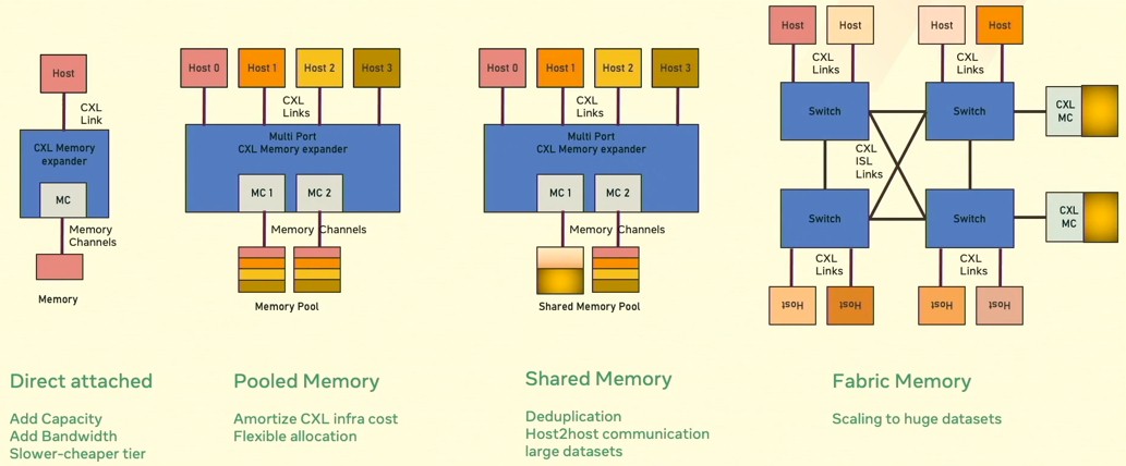
“The first generation of CSL memory products will include memory modules that are directly attached to CPU root ports,” Chauhan. “They will likely be CXl 1.1 compliant with some CXL 2.0 features, and will bring the capabilities of adding memory capacity or memory bandwidth or support for lower cost media types in the system. The second generation of products will include full CXL 2.0 support and will allow memory pooling, which has the promise of reducing the overhead costs of CXL infrastructure, like the boards and ASICs that are needed to attach memory. Additionally, this will also allow making flexible allocations on an as-needed basis to avoid static overprovisioning of memory on each host. The third generation of products will leverage capabilities introduced in CXL 3.0, such as coherent sharing of CXL-attached memory. This will enable applications to scale up using shared memory communications and reduce memory footprints by keeping one copy of the working data set as opposed to replicating it on all compute nodes. In the fourth generation, we will see products that will take full advantage of CXL 3.0 features, such as multiple levels of switching, to support large datasets and large scale disaggregation of memory from compute, as well as scaling up the very large datasets across a large number of compute nodes.”
Such clustering at the memory level will not be as tight as symmetric multiprocessing (SMP) from days gone by in server architectures, and they will even be looser than the non-uniform memory access (NUMA) interconnects that are common in server architectures today. But this kind of memory fabric will also be as fat as any InfiniBand or Ethernet interconnect and lower latency as well, end to end, by definition if PCI-Express switch makers (that would be Broadcom and MicroChip) can grow the radix of their devices and keep the latency down.
But even more interesting in this hierarchy shown on the right side of the chart above is the ability to disaggregate compute engines and memory and to bring whatever kind of compute to the data over the PCI-Express switch fabric and the fabric manager controlling the links between all devices. In theory, with PCI-Express 3.0. up to 4,096 devices can be linked together in a fabric, and as we have already pointed out, that is a fairly large clustered system for most organizations. And that device count will no doubt go up over time, too.
None of this is perfect, of course. But we were never going to get enough memory controllers to drive up memory bandwidth and capacity anyway. Not where it needs to be.
We can stop-gap with PCI-Express memory and CXL for now, and as many have suggested, follow IBM’s lead on OpenCAPI memory and eventually move to differential DIMMs and generic SerDes for I/O and memory and then configure and reconfigure compute engines for I/O and memory as we see fit. If we need a compute engine with very high bandwidth, we can use HBM, and if we need higher capacity and lower latency than is available over CXL 4.0 or CXL 5.0 atop PCI-Express 7.0 and PCI-Express 8.0 – well, you can pay a premium for a dedicated DDR6 or DDR7 controller chiplet and add it to the compute engine package. Adding more – a lot more – PCI-Express lanes to future compute engines seems like a better idea, particularly given the high power and high pin counts referenced above.
We shall see what customers tell chip makers to do, and if they will listen.

The Ticking And Tocking Of Intel’s “Ice Lake” Xeon SP
It has been a long time since Intel changed its manufacturing process – what it used to call a “tick” – and the microarchitecture and architecture of a processor design – what it used to call a “tock” – at the same time. But with the fourth generation “Ice Lake” …
Ethernet Consortium Shoots For 1 Million Node Clusters That Beat InfiniBand
Here we go again. Some big hyperscalers and cloud builders and their ASIC and switch suppliers are unhappy about Ethernet, and rather than wait for the IEEE to address issues, they are taking matters in their own hands to create what will ultimately become an IEEE standard that moves Ethernet …
Putting TACC’s “Stampede3” Through The HBM Paces
When you host the workhorse supercomputers of the National Science Foundation, you strive to provide the best possible solutions for your scientists. The Stampede and Frontera systems at the Texas Advanced Computing Center (TACC) at the University of Texas at Austin have been those workhorses. TACC continues to get National …
Be the first to comment