

Let the era of 3D V-Cache in HPC begin.
Inspired by the idea of AMD’s “Milan-X” Epyc 7003 processors with their 3D V-Cache stacked L3 cache memory and then propelled by actual benchmark tests pitting regular Milan CPUs against Milan-X processors using real-world and synthetic HPC applications, researchers at RIKEN Lab in Japan, where the “Fugaku” supercomputer based on Fujitsu’s impressive A64FX vectorized Arm server chip, have fired up a simulation of a hypothetical A64FX follow-on that could, in theory, be built in 2028 and provide nearly an order of magnitude more performance than the current A64FX.
AMD let the world know it was working on 3D V-Cache for desktop and server processors back in June 2021, and showed off a custom Ryzen 5900X chip with the stacked L3 cache atop the die, tripling its capacity with only one stack. (The stacked L3 is twice as dense because it doesn’t have any of the control circuitry that the “real” L3 cache on the die has; the stacked cache, in fact, piggybacks on the on-die cache pipes and controllers.) Last fall, ahead of the SC21 supercomputing conference, AMD unveiled some of the features of the Milan-X SKUs in the Epyc 7003 CPU lineup, and the Milan-X chips were unveiled in March of this year.
We think that 3D V-Cache is going to be used on all processors, eventually, once the manufacturing techniques are perfected and cheap enough, and precisely because this will free up die area to be dedicated to more compute cores. (We discussed this, among other things, in an interview with Dan McNamara, senior vice president and general manager of the server business at AMD.
The researchers at RIKEN, working with colleagues at Tokyo Institute of Technology and the National Institute of Advanced Industrial Science and Technology in Japan, KTH Royal Institute of Technology and Chalmers University of Technology in Sweden, and the Indian Institute Of Technology, got their hands on servers with AMD Epyc 7773X (Milan-X) and Epyc 7763 (Milan) processors, and ran the MiniFE finite element proxy application – one of the important codes used by the Exascale Computing Project in the United States to test the scale of exascale HPC machines – on the two machines and showed that the extra L3 cache helped boost performance by a factor of 3.4X. Take a look:
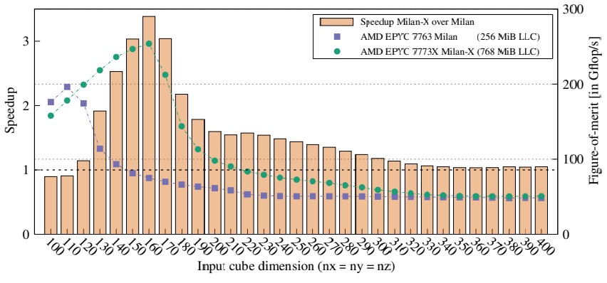
In the HPC world, 3.4X is nothing to shake a stick at. And that got the RIKEN team to thinking: What would happen if 3D V-Cache was added to the A64FX processor? And more specifically, that got them to noodling about how they might marry 3D V-Cache to a hypothetical kicker to the A64FX, which would be expected in around six years or so based on the cadence between the “K” supercomputer using the Sparc64-VIIIfx processor from 2011 and the Fugaku supercomputer based on the A64FX from 2020. And so they fired up the Gem5 chip simulator and simulated what a future A64FX kicker with a large L2 cache (the A64FX does not have a shared L3 cache, but does have a large shared L2 cache), which it is subbing LARC for large cache, might look like and how it might perform on RIKEN codes and popular HPC benchmarks.
This is the power of creating digital twins, aptly illustrated. And if you read the paper put out by RIKEN and its collaborators, you will see that this task is not as smooth as it seems in the Nvidia and Meta Platforms advertisements, but that it can be done sufficiently well to get a first order approximation to compel funding in future research and development.
We have done many deep dives on the technology in the Fukagu system, but the big one is this piece in 2018. And this die shot of the A64FX processor is a good place to start the discussion about the hypothetical A64FX kicker CPU:
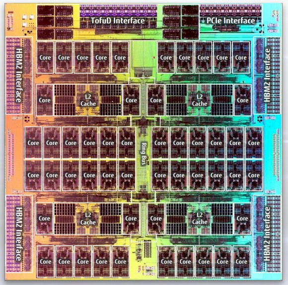
The A64FX has four core memory groups, or CMGs, which have custom Arm cores created by Fujitsu 13 cores, a chunk of shared L2 cache, and an HBM2 memory interface. One of the cores in each group is used to manage I/O. which leaves 48 cores that are user addressable and does the calculations; each core has a 64 KB L1 data cache and a 64 KB L1 instruction cache, and the CMG has an 8 MB segmented L2 cache, with 32 MB slices per core. The design does not have an L3 cache, and that is on purpose because L3 caches often cause more contention than they are worth, Fujitsu has always believed in the largest possible L2 caches in its Sparc64 CPU designs, and the A64FX carries this philosophy forward. The L2 cache has 900 GB/sec of bandwidth into the cores in each CMG, so the aggregate L2 cache bandwidth across the A64FX processor is 3.6 TB/sec. Each A64FX core can do 70.4 gigaflops at 64-bit double precision floating point, which is 845 gigaflops per CMG and 3.4 teraflops across the whole processor complex, which is etched in a 7 nanometer process by Taiwan Semiconductor Manufacturing Co.
Believe it or not, RIKEN did not have the floorplan of the A64FX processor, and had to estimate it from die shots and other specs, but it did that as the starting point for the Gem5 simulator, which is open source and used by a lot of tech companies. (There is no way this estimate was done without Fujitsu’s approval and review, however unofficial, and therefore we think the floorplan used for the A64FX is absolutely accurate.)
Once it had that A64FX floorplan, the RIKEN team assumed that a 1.5 nanometer process would be available for a shipping processor in 2028. What that dramatic shrink allows is for the CMG in the LARC hypothetical chip to be one quarter the size of the one used in the A64FX, which means the LARC processor can have 16 CMGs. Assuming that the L2 cache can be shrunk at a similar pace and scale, the idea with the LARC chip is to have eight L2 cache dies with through chip interfaces (TCIs) gluing them all together, similarly to the way through-silicon vias (TSVs) are used in HBM memory stacks. RIKEN thinks that this stacked memory can run at around 1 GHz, based on simulations and other research on stacked SRAM, and as you can see from the comparative CMG diagrams below, it thinks that it can create stackable L2 SRAM chips that cover the entirety of the CMG:
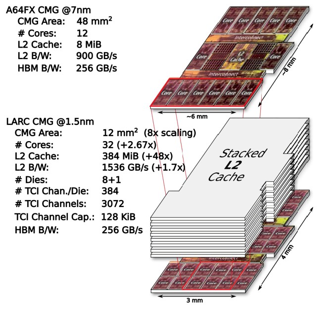
This is an important distinction, since AMD’s 3D V-Cache only stacks L3 cache on top of L3 cache, not compute dies. But we are talking about 2028 here, and we have to figure the materials people will figure out the heat dissipation issues of having L2 cache on top of CPU cores. Running at 1 GHz, the bandwidth on the L2 cache in the LARC’s CMG will be 1,536 GB/sec, which is a factor of 1.7X faster than on the A64FX, and the cache capacity will be 384 MB per CMG or 6 GB across the socket. Moreover, RIKEN figures that the CMG will have 32 cores, which is a factor of 2.7X higher.
To isolate the effect of the stacked L2 cache on the LARC design, RIKEN kept the HBM2 memory at the HBM2 level and did not simulate what HBM4 might look like and kept the HBM memory capacity the same at 256 GB. We wonder if the CMGs with such high L2 cache bandwidth might not be constrained by the HBM2 bandwidth and what might happen to the overall performance of a 512-core LARC socket might be inhibited by that relatively low HBM2 bandwidth and low capacity (only 8 GB per CMG). But sticking with HBM2 with one controller per CMG and having 16 CMGs on the LARC, that is only 128 GB of HBM2 memory and 4 TB/sec of bandwidth per LARC socket. A factor of 4X improvement will probably be in order for the real LARC design, we guess, to keep it all balanced, assuming the clock speed on the cores and uncore region doesn’t change much.
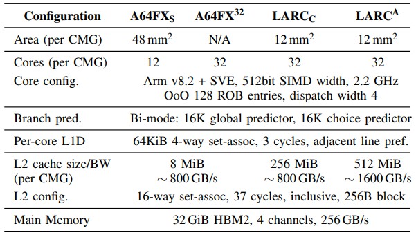
To isolate the effect of the core differences, the RIKEN researchers ginned up a 32-core CMG, but left the cache size a 8 MB per CMG and 800 GB/sec of bandwidth. And just for fun, they created a LARC design with 256 MB of L2 cache and the same 800 GB/sec of bandwidth (presumably with only four L2 stacks) to isolate the effect of capacity on HPC performance and then did the full on 512 MB of L2 cache running at 1.5 GB/sec. By the way, the LARC cores are the same custom 2.2 GHz cores used in the A64FX – no changes here, either. And you know full well that by the time 2028 rolls around, Fujitsu, Arm, and RIKEN will have a radically better core but it may not have better 512-bit vectors. (We shall see.)
Here is how the hypothetical LARC and actual A64FX chips measured against each other in the STREAM Triad memory bandwidth benchmark test:
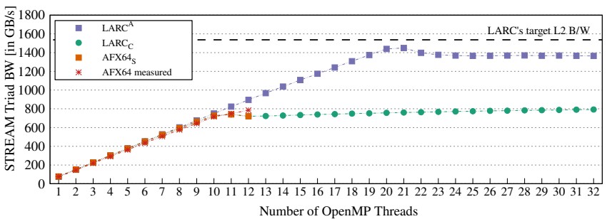
That test shows bandwidth as the number of OpenMP threads increases, and the one below shows how STREAM performance changes with the size of the vector input data from 2 KB to 1 GB.
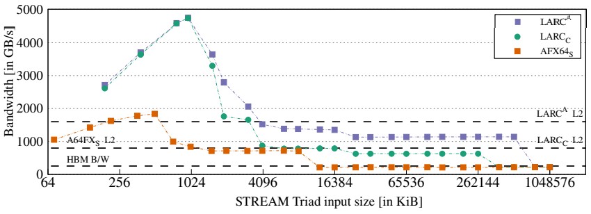
The spike in the LARC lines is because with 2.7X times the cores within a CMG, you also have 2.7X the amount of L1 cache, so the smaller vectors all fit in L1 cache; and then the larger vectors can now fit into L2 cache for a long time. So the simulated LARC chip just kicks it in until all of this cache runs out.
Here is the important thing after all that simulating. Across a wide suite of HPC benchmarks, including real applications running at RIKEN and other supercomputer centers as well as a slew of HPC benchmarks we all know, the LARC CMG was able to deliver around 2X more performance on average and it was as high as 4.5X for some workloads. Couple this with a quadrupling of CMGs and you are looking at a CPU socket that could be on the order of 4.9X to 18.6X more powerful. The geometric mean of performance improvements between A64FX and LARC for those applications that are sensitive to L2 cache is 9.8X.
By the way: The Gem5 simulations were run at the CMG level because the Gem5 simulator could not handle the full LARC socket with sixteen CMGs, and RIKEN has had to make some assumptions about how that scale would work out within the socket.

Hope Springs Eternal For Arm Servers
IT organizations are funny creatures, indeed. On the one paw, they are eternally optimistic about the prospects for new technologies, and on the other paw, they are extremely resistant to change because of the economic and technical risks that change requires. For more than a decade now, the people who …
Isambard 2 Is About Driving Technology Diversity
It’s been just more than a decade since Arm executives began to talk about bringing the company’s system-on-a-chip (SoC) architecture, which has long been the dominant design for processors found in billions of smartphones and other mobile device, into the datacenter. They boasted that within years they would be chipping …
HPC Pioneers Pave The Way For A Flood Of Arm Supercomputers
Over the past few years, the Arm architecture has made steady gains, particularly among the hyperscalers and cloud builders. But in the HPC community, Arm remains under-represented. But perhaps not for long. The “Fugaku” system at RIKEN Lab in Japan is without a doubt the largest and best known Arm …
Be the first to comment