

Designing a great CPU or GPU, or even an FPGA or a custom ASIC like a switch or router chip, is an important aspect of creating ever-more-powerful systems. But how these components, which are being broken into chiplets to increase yields and reduce cost, fit together within a package and across packages and nodes is equally important. And at the Computex conference in Taiwan this week, AMD was showing off some of its prowess with both chip process and chip process and chip packaging and how advances in both realms are the key to AMD’s expansion in all high performance computing markets, not just the simulation and modeling ones.
“At AMD, we are always thinking about what’s next,” explained Lisa Su, chief executive officer at the company in her Computex keynote address, the third year in a row that she was asked to give one (which you can see at this link). “Advanced technology is a key foundation of our product leadership, and that means putting the best process technology together with the best packaging technology. We were early adopters of 7 nanometer advanced manufacturing technology from TSMC, and by now we have delivered more than 30 products in 7 nanometer across all of our markets. And our roadmap to 5 nanometer technology is right on track, including our first Zen 4 products, which will be available next year.”
Su reminded everyone that AMD has also been on the forefront of chip packaging techniques, which we have always believed were as important as chip design and chip process. You have to be good at all three to succeed – or partner with those who are doing the primary research and can develop it into the future technologies that you will need. IBM used to be good at all three, back in the day, and AMD has done a good job in doing research on various kinds of chip packaging while at the same time keeping an eye on the chip process advances that it used to be part of before it spun out the GlobalFoundries in early 2009.
“We are also the leaders in advanced packaging technology,” Su said. “Our investments in innovation in packaging have been a multi-year, multi-technology journey. In 2015, AMD introduced high bandwidth memory, or HBM, and silicon interposer technology to the GPU market, which led the industry for memory bandwidth in a small form factor. We then set a new performance trajectory for compute in the datacenter and PC markets in 2017 when we introduced high volume multichip module packaging. And in 2019, we introduced chiplets, using different process nodes for the CPU cores and the I/O in the same package, which enabled significantly higher performance and capabilities.”
It was always a matter of time before chips would move more solidly into the third dimension. Chips are not really flat objects, 2D objects, but have dozens of layers of materials stacked up to create their transistors and circuits. But eventually, because of the limitations of the reticle size of lithographic equipment and the high cost of making a big chip compared to the lower cost of making many chiplets in the same area (the yields are statistically better on the smaller chips so the number of wafers it takes to get a certain amount of raw compute is smaller, which drives down the cost), we all knew that we would go 2.5D (with chips linked to each other over interposers to a full-on-3D stacking of dies to create much more compact devices that have all sorts of benefits.
This is where, Su hinted in her keynote, AMD is going: Up.
“We have worked closely with TSMC on their 3D fabric to combine chiplet packaging with die stacking to create a 3D chiplet architecture for future high performance computing products.”
The first prototype chip that AMD is working on with Taiwan Semiconductor Manufacturing Corp that will use the 3D fabric is a vertical cache. In the prototype, AMD took a Ryzen 5000 series processor and stacked a 64 MB SRAM implemented in 7 nanometers directly on top of each of the core complex dies, or CCDs, and this tripled the amount of L3 cache feeding the cores. The 3D cache is bonded directly to the Zen3 CCD with through silicon vias, which pass signals and power between the stacked chips, pushing more than 2 TB/sec of bandwidth.
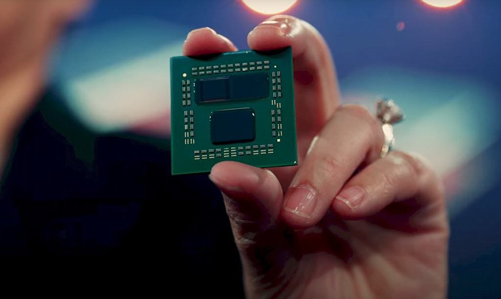
The production chip that Su was showing off was a Ryzen 5900X CPU with 3D V-Cache, which had 96 MB of cache per CCD, for a total of 192 MB of L3 cache across Ryzen processor complex with 12 or 16 cores. That is what is shown here:
On benchmark tests running the Gears V video game, the plain vanilla Ryzen 9 5900X could drive 184 FPS, while the prototype Ryzen 5900X with 3D V-Cache could drive 206 FPS. Both at same core count (it was not specified) and both ran at the same 4 GHz clock speed; this yielded a 12 percent performance increase on Gears V. Across a suite of games, the average performance boost was 15 percent. As Su correctly put it, this is a performance boost that is equivalent to an architectural generation step in CPU design – without actually having to change the CPU cores or I/O dies.

Su said that the 3D fabric technique created by TSMC and implemented with a lot of help by AMD has over 200X the interconnect density of 2D chiplets, and 15X higher density than other 3D stacking techniques. Incidentally, this is a direct copper-to-copper wire bond with no solder bumps at all, and this 3D fabric technique is greater than 3X more energy efficient per signal compared to microbump 3D packaging approaches.
“All of these things make this truly the most advanced and flexible active on active silicon stacking technology in the world,” she added with a smile.
Su said that 3D V-Cache will be in production at the end of this year. We are hoping that it will tested out in server CPUs soon, perhaps with the “Trento” custom CPUs to be used in the 1.5 exaflops “Frontier” supercomputer being installed later this year at Oak Ridge National Laboratory.
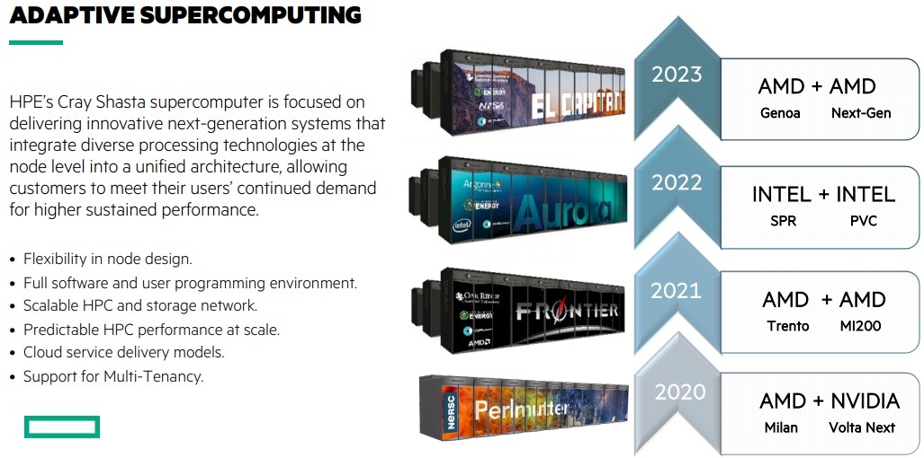
Not much is known about Trento, but it is widely expected to be a custom “Milan” part that takes the same cores as are used in Milan but marries them to a new I/O and memory chiplet that has Infinity Fabric 3.0 links on the port, and enough of them so that the CPU memory of a single socket and the memory of four GPUs can be all linked together into a single, coherent, shared memory. Oak Ridge has coherent memory in the IBM Power9 CPU-Nvidia Volta GPU compute complexes that are the basis of the “Summit” supercomputer, and this coherence, enabled by the addition of NVLink ports on the Power9 processors, was one of the salient characteristics of the architecture that allowed IBM and Nvidia to win the deal to build Summit. There is no way Oak Ridge would award the Frontier system to any vendor that didn’t have such coherence in their CPU and GPU complexes.
If the Instinct MI200 GPU accelerator is, as many suspect, a 5 nanometer shrink of the “Arcturus” MI100 GPU that puts two chiplets or two whole GPUs in a single socket, as many suspect, then the number of Infinity Fabric 3.0 ports that will be needed to make the CPU and GPU memories coherent (without too many latency-inducing hops between devices) will be large, and thus we expect that the Trento I/O and memory die will be large, too. There is an outside chance that the Trento chips could support PCI-Express 5.0 peripherals and DDR5 buffered main memory. No one seems to know for sure outside of Hewlett Packard Enterprise, the prime contractor for the machine, AMD, and Oak Ridge. But what we do know is that they are all keen to get Oak Ridge into the field with Frontier on time, before the November 2021 Top 500 rankings, so the United States can claim exascale supremacy ahead of China.
We shall see. You can bet China wants to steal that thunder in the June 2021 Top500 rankings.
We think it would be interesting if Trento also sported much fatter caches with the 3D V-Cache technique, and in fact we will be surprised if this is not part of the package. If it isn’t, you can bet Pat Gelsinger’s last dollar that it will be part of the “Genoa” Epyc 7004 kicker to the Milan Epyc 7003s.

Eni Chooses Utility Pricing For New HPC4+ Supercomputer
Here are two things you don’t see every day in the realm of scientific and technical high performance computing. The first thing is seeing an organization upgrade an existing system after it has already had its successor plopped down in the datacenter next to it. And the second thing is …
For CPU Makers and OEMs Alike, It’s A Platform View
Dell took a look at the two weeks between the rollouts by AMD and Intel of their latest server processors and, after some debate, decided to unveil its entire portfolio of new and enhanced systems – featuring the new chips from both vendors – at the launch of AMD’s latest …
AMD’s Instinct GPU Business Is Coiled To Spring
Timing is a funny thing. The summer of 2006 when AMD bought GPU maker ATI Technologies for $5.6 billion and took on both Intel in CPUs and Nvidia in GPUs was the same summer when researchers first started figuring out how to offload single-precision floating point math operations from CPUs …
Be the first to comment