

When the top brass at Intel say that the “Sapphire Rapids” Xeon SP CPUs and “Ponte Vecchio” Xe HPC GPUs that are coming out early next year represent the “largest architectural shift in over a decade,” they ain’t kidding. At the third annual Architectural Day hosted this week, we heard that time and time again, and importantly for Intel’s financial and technical future and for increasing the level of competition for datacenter compute and networking silicon, it looks like it is actually true.
This reminds us of a wise phrase that we learned a long time ago from the former corporate controller at Chesebrough-Ponds (acquired by Unilever back in the late 1980s) who also taught accounting and finance in his later years. To quote: “The best time to do anything was ten years ago. The second-best time is right now.”
There’s not a lot of room for guilt or sadness or despair in that phrase; it’s about action. Such a forward-looking sentiment is one that Intel has desperately needed for about a decade and one that Raja Koduri, Intel’s chief architect and now head of its new Accelerated Computing Systems and Graphics Group, has brought to the company more than anyone else. More than Intel prodigal son, Pat Gelsinger, who has returned as Intel chief executive officer to help call the broader Intel plays in the markets where the chip maker has game. They are both optimistic technologists, and they also know how to get chip done.
While there were some revelations at the Architecture Day, which we will be going through in the coming days – a deep dive on the two-cycle “Gracemont” Efficient Core and “Golden Cove” Performance Core CPU engine designs, the modular Xe graphics chip design, as well as on the custom “Mount Evans” DPU that the company has designed and is building (using Arm cores no less) for a “top cloud provider” – what we want to focus on right now is Sapphire Rapids and Ponte Vecchio, which are the two most important datacenter components that will be coming out of Intel and which demonstrate the strategy that the company will be taking to create compute engines in the next decade. They are also the heart of the much-delayed “Aurora” supercomputer at Argonne National Laboratory.
Yes, it would have been better had Intel developed and embraced its chip packaging techniques a decade ago, before Moore’s Law process shrinks had started slowing and as Dennard scaling of clocks had already been dead for ten years. It would have surely been better to see these signals and do something about it then, before it was a big problem. But, the second-best time is to do it right now. And, to Intel’s credit, it is finally doing that and we are going to get some real competition between Intel, AMD, and Nvidia in the coming years on a lot of different fronts. This is good for every datacenter in the world.
We will start with Sapphire Rapids, and then follow up separately with an overview of what we now know about Ponte Vecchio, and then do the deep dives on the CPU and GPU compute architectures.
Shooting Through Sapphire Rapids
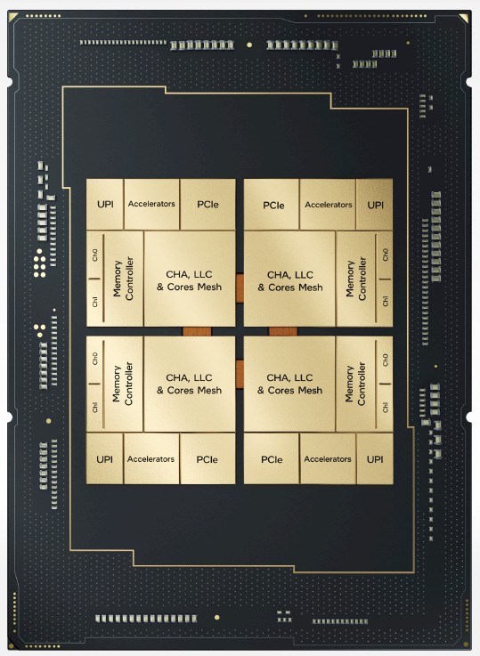
The two most important things you need to know about Sapphire Rapids is that it will be using the new Performance Core, formerly known as Golden Cove, and that it is a four-chip module using Embedded Multi-die Interconnect Bridge (EMIB) links between the chips.
We will probably not refer to the basic unit of compute on Sapphire Rapids and its follow-ons as a P-Core unless everyone else starts doing it to contrast it with the Efficient Core, or E-Core, formerly known as the Gracemont Atom core. Intel has had a big and little core strategy for a long time, but we do expect that sooner or later there will be a mix of core types in a Xeon SP package as well as a mix of memory types. The Core client processors starting with “Alder Lake” will have a mix of P-Core and E-Core compute. (OK, so that is convenient shorthand.)
If you look at the Sapphire Rapids package above, this is roughly analogous to the approach that AMD took with its first generation “Naples” Epyc chips, which interlinked four Ryzen desktop chips with a HyperTransport-infused PCI-Express interconnect called Infinity Fabric. By doing this, Intel can get away from a monolithic chip design that is hard to get good yields on with its second rev 10 nanometer process and therefore lower the overall cost of the Sapphire Rapids socket even though the interconnect and packaging overhead is not free.
What we think is odd, and what we will be asking about in the future, is why Intel did not pull out the memory controllers and I/O controllers and centralize these into a hub chip like AMD did in the “Rome” Epyc 7002 and “Milan” Epyc 7002 chips. EMIB looks more like an extender for the on-chip mesh network that Intel has used since the “Skylake” Xeon SP designs to link cores, caches, caching and home agents (CHA), and snoop filters (SF). That mesh network was first used in the “Knights Landing” Xeon Phi processor made of vector-enhanced Atom cores way back in 2015 and came into the Skylake design to replace the ring interconnects that formerly lashed the cores and caches on the many variants of the Xeon E5 and Xeon E7 chips for many generations.
What this means is that Intel can make a high-end workstation chip aimed at performance desktops with, say, ten cores and lash four of these together to create a 40 core chip that looks and smells like an improved “Ice Lake” monolithic chip to operating systems. It can do away with the XCC or Extreme Core Count 28-core die and the UCC or Ultra Core Count 40-core die, which has to be very expensive to build compared to chips with eight or ten cores. No one knows, as yet, what the die core counts will be with the tiles used in the Sapphire Rapids package, but Intel will want as few as possible variations and as many cores as possible in the full configuration. We think a dozen cores per tile is a likely number, and sixteen cores per tile would be even better if it can be done in the 10 nanometer process and not create a 400 watt part. This would ramp the Sapphire Rapids socket to 48 cores or 64 cores max, the latter toe to toe with AMD’s Epyc 7002 and 7003 chips. The rumor is that the socket will deliver 56 cores, or 14 per tile. We strongly suspect that there might be 16 cores on the die and that two are being sacrificed to the Yield Gods.
We wonder if there is a NUMA latency penalty by linking at the mesh instead of at the memory controllers. Nevine Nassif, chief engineer of the Sapphire Rapids package, talked a little bit about this in her presentation at Architecture Day.
“At the heart of Sapphire Rapids is a new modular, tiled architecture that allows us to scale the bounds of the Xeon architecture beyond the physical reticule,” Nassif explained. “Sapphire Rapids is the first Xeon product built using EMIB, our latest 55 micron bump silicon bridge technology. This innovative technology enabled independent tiles to be integrated in the package to realize a single, logical processor. The resulting performance, power, and density are comparable to an equivalent monolithic die. We are now able to increase core counts, cache, memory, and I/O free from the physical constraints that would otherwise have been imposed on the architecture and that would otherwise have been imposed on the architecture and led to difficult compromises. This base SoC architecture is critical for providing balance, scaling, and consistent performance across all workloads, and is key for achieving datacenter scale, elasticity, and achieving optimal datacenter utilization. With this architecture, we are now able to provide software with a single, balanced, unified memory access, with every thread having full access to all resources on all tiles, including cache, memory, and I/O. The result is consistent low latency and high cross-sectional bandwidth across the entire SoC, and is one of the critical ways we provide low jitter in Sapphire Rapids. While Sapphire Rapids delivers out of the box scalability for existing software ecosystems, users can enable clustering at sub-NUMA and sub-UMA levels for additional performance and latency improvements.”
There have been latency penalties on the XCC and UCC Xeon SP dies, causing Intel to carve them up into virtual NUMA regions to boost performance, and it looks like this will be no different. Our guess is that in many cases, software will look at this as four processes rather than one. We shall see what the real deal is when someone tries to scale a VMware ESXi virtual machine across more than one tile. This is what really sent the Naples Epycs into a tizzy.
Each of the four tiles on the Sapphire Rapids package has a DDR5 memory controller with two channels and more than 25 MB of last level cache, which almost certainly is an L3 cache that is shared across all tiles that will weigh in at more than 100 MB and which will be fed by a total of eight DDR5 channels. The chip will also support “Crow Pass” Optane 300 Series persistent memory, which Intel previewed last December.
On the I/O front, each Sapphire Rapids tile will have a single x24 (24 lane) UltraPath Interconnect (UPI) port for cross-coupling to other Sapphire Rapids sockets to create NUMA machines with two, four, or eight sockets. These UPI links will run at 16 GT/sec. The “Ice Lake” Xeon SP chip was only available for machines with one or two sockets and had three UPI links running at a slower 11.2 GT/sec. The “Cascade Lake” Xeon SPs had only two UPI ports and ran at 10 GT/sec. The Sapphire Rapids chips will sport a single PCI-Express 5.0 port per tile, and therefore four across the socket; Intel has not said how many lanes of PCI-Express 5.0 the socket will deliver. The Ice Lake server chip had 60 lanes running at PCI-Express 4.0 speeds, which had half the bandwidth per lane; the word on the street is that the entire chip will support 80 lanes, so that is 20 lanes per tile. That PCI-Express 5.0 controller will support the CXL 1.1 coherency protocol for linking to accelerators and external memory.
We already talked about this back in June, but Intel is also offering an HBM memory option on selected Sapphire Rapids CPUs aimed at HPC and AI workloads that need more memory bandwidth than DDR5 can deliver. The word on the street back in June is that Intel was going to be very aggressive, delivering four stacks of HBM2 memory, four high at 4 GB per chip, for a total of 64 GB per socket.
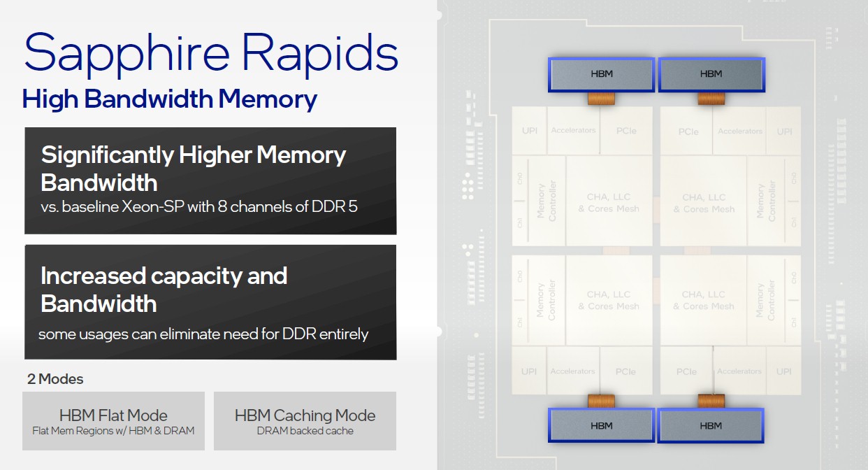
This HBM memory will be available in two modes (well, three we think). The first is called flat mode, which carves up the memory into HBM and DDR regions and then a caching mode, which uses the DDR5 memory as a kind of cache for the HBM memory. Of course, you can just load it up with HBM and not use any DDR5 memory at all, which will be the third way. It would be very interesting to see a fourth way, which would provide coherency across the HBM memory in a Sapphire Rapids CPU and the HBM memory in the Ponte Vecchio GPU accelerator over CXL links – and we think this will happen in the Aurora system at Argonne.
At the Architecture Day event, Intel gave some hints about how the Sapphire Rapids processor would perform relative to itself in different modes and to its predecessors as well.
The first chart is just raw 8-bit integer (INT8) performance, which is used for machine learning inference in a lot of neural networks these days. Take a look at this:
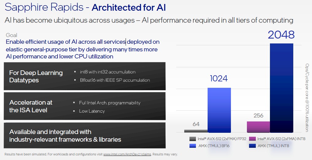
The Advanced Matrix Extensions, or AMX, instructions added with the Golden Cove core are clearly going to significantly boost inference performance. This chart shows operations per cycle, so AMX, which we think is a matrix math overlay for AVX-512 units, will grow INT8 performance by a factor of 8X compared to Ice Lake (or just using the INT8 functions raw in the VNNI instructions added with Cascade Lake and Ice Lake chips). Bfloat16, also used for AI training and inference, will run at half this rate, of course.
We did a more detailed analysis of AMX here, and spoke to Intel separately from its Architecture Day to get some insight into the motivations behind AMX.
The second performance claim has to do with microservices performance – meaning massively distributed applications that are common here in the cloud era.
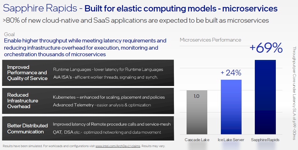
It looks like raw instructions per clock (IPC) will be about 19 percent higher with Sapphire Rapids compared to Ice Lake, and Ice Lake was 20 percent higher than Cascade Lake on raw IPC, so these numbers are consistent. It’s about 25 percent higher than you would expect based on IPC alone, in fact. Faster memory, more I/O, and a zillion other tweaks all contribute to this, of course.


The Killer Apps For FPGAs Could Be SmartNICs And Storage
If FPGAs are going to take off in the datacenter in their own right, they are going to need their own killer apps. Plural. At The Next FPGA Platform event that we hosted recently in San Jose, there was plenty of talk about how FPGAs have been embedded in all …

Will Open Compute Backing Drive SIOV Adoption?
Virtualization has been an engine of efficiency in the IT industry over the past two decades, decoupling workloads from the underlying hardware and thus allowing multiple workloads to be consolidated into a single physical system as well as moved around relatively easily with live migration of virtual machines. It is …
Intel To Broaden FPGA Lineup And Make Them At Home
Back in 2015, when Intel was flush with cash thanks to a near-monopoly from X86 datacenter compute, it shelled out an incredible $16.7 billion to acquire FPGA maker Altera because a few hyperscalers and cloud builders were monkeying around with offloading whole chunks of CPU compute to FPGAs to create …
The four stacks of HBM would add 32 memory channels of 128 bits on Sapphire Rapids. Someone mentioned that Aurora is using this.
I think this makes more sense than moving from 8 to 12 channels on the leaked zen4 genoa design.
With Intel’s emphasis on ai processing, it might be the only way to get past the memory controller bottleneck.