

Newly anointed Intel chief executive officer Pat Gelsinger held the coming out party for his strategy to get the world’s largest chip manufacturer and designer back on track, called “Intel Unleashed: Engineering The Future,” on Tuesday after the market closed.
It was a strange echo of an essay we wrote back in October 2020, called Intel Needs To Engineer Its Financial Future, where we pointed out that Intel needs to engineer its financial future, or better still, finance its engineering future, not financially engineer its future, and that the $9 billion from SK Hynix acquisition of Intel’s flash business should be used to make a fab that in turn makes fabulous chips.
This is basically what Intel is doing, as it turns out. And more.
Like many, back in January as Geisinger was brought back to the chip maker for his “ideal job,” we had been expecting for Intel to do something radical with its foundry business, perhaps spinning it off with the support of the US government, which is beginning to see the effect on the government agencies itself and on the US economy overall as supply chain issues, including but not limited to effects from the coronavirus pandemic and from shortages in substrates used to etch transistors onto silicon wafers, cause shortages and delays in deliveries of all kinds of chippery.
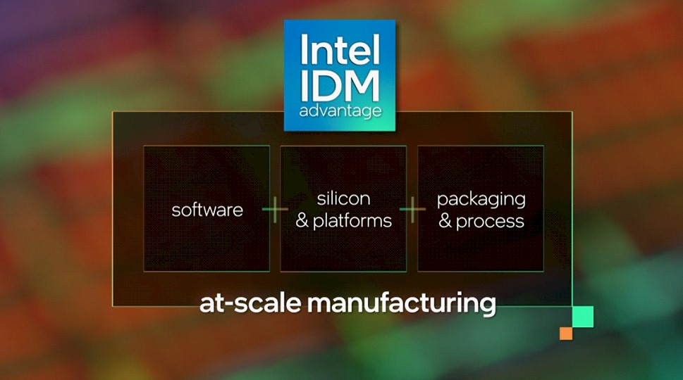
Rather than a foundry spinoff, Intel is doing a foundry spin-in, setting up a separate business unit within the company, called Intel Foundry Services, that will have its own profit and loss statements like other Intel divisions and which will have Randhir Thakur as its president. Thakur is currently in charge of Intel’s own supply chain operations, and this does not mean buying pencils and paperclips, but rather buying all of the complex equipment that goes into the foundries and staging chips from development to design to manufacturing to distribution to customers, a job that Thakur has held since November 2017. During the dot-com boom, Thakur was a senior executive at semiconductor manufacturing equipment maker Applied Materials, then he did a three-year stint at SanDisk managing flash memory manufacturing and testing and other supply chain and procurement related to this, and then during the Great Recession he returned to Applied Materials to run its solar cell fab and then became general manager of its Silicon Systems Group. So Thakur seems like a good choice to run Intel’s foundry business, which has been around for years but as Gelsinger admitted on the call with Wall Street analysts, was not something that Intel put a lot of heart into.
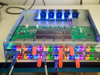
No one really believed that Intel was going to open up its foundry, and Intel really didn’t. But this time around, according to Gelsinger, Intel is dead serious, starting with a $20 billion investment in two chip fabs in its Ocotillo campus in Chandler, Arizona. This is where Fab 42, which is shown in the feature image above is located, and also where Intel’s ill-fated 10 nanometer manufacturing processes are operating in production (finally). Intel is not being precise about what these two foundries will be doing, but Gelsinger confirmed that they would be doing extreme ultraviolet, or EUV for short, lithography techniques and that means 7 nanometer or smaller transistor geometries. Gelsinger added that the company would be expanding foundry capacity elsewhere in the United States and in Europe, and would be making announcements about when and where before the end of the year.
It will be hard for many to take Intel seriously as a merchant foundry, but with demand for chip making exceeding supply in the world and geopolitics also creating a certain amount of heartburn with 80 percent of advanced foundry capacity being located in Taiwan and China and only 15 percent in the United States and 5 percent in Europe, it is no surprise that Intel will be able to capitalize on this political climate, getting support from the United States (in the states of Arizona, Massachusetts, New Mexico, and Oregon), in Israel (in Jerusalem and Kiryal Gat), and Ireland (in Leixlip). Intel also has a foundry in Dalian, China, so it is contributing to the chip imbalance that it is trying to capitalize on.
Intel has test and assembly sites in two locations in the United States, two in China, two in Malaysia, one in Costa Rica, and one in Vietnam, and frankly, while Gelsinger spent a lot of time talking about the “supply chain” issues (meaning national security issues) with the current geographic distribution of foundries, the same logic should hold for test and assembly factories. A wafer is perfectly useless until it is cut into chips and put into packages and proven to be a good part, after all.
While specifics were not given out, Gelsinger said that Intel was expecting to receive incentives from the Biden administration for building out indigenous fab capacity here in the United States and also incentives from the state of Arizona for the $20 billion foundry buildout revealed today. Not that Intel needs it, apparently.

“This is the Intel strategy, period. Full stop,” declared Gelsinger. “It does not depend on a penny of government support or state support or any other investments to make it successful. It is the right strategy for us going forward,” he said, adding that “of course, governments – we want incentives. We want investments because it is the right thing for them to accelerate manufacturing and this imbalance of the global supply chain. But we’re making these commitments without any commitments from the governments to accelerate them.” Intel is, as Gelsinger punned it, “putting our chips on the table” first and then anticipating that eager governments will up the ante some.
The opening up of the foundry operations includes not only working with IBM on a partnership for research in advanced chip manufacturing and design processes, but also simplifying and tweaking its own chip making tools so they can be used at other fabs such as rivals Taiwan Semiconductor Manufacturing Corp (primarily in Taiwan and China but adding a foundry in Arizona with construction starting this year), Samsung Electronics (in Taiwan), GlobalFoundries (primarily in the US and Europe), and United Microelectronics Corp (in Taiwan, Singapore, China, and Japan). Intel is also working with Cadence and Synopsys to tweak its tools to work better with Intel processes, ranging from 22 nanometer to 7 nanometer and smaller, and has committed to making its tools suitable for the manufacturing of processors based on X86, Arm, and RISC-V cores.
(In hindsight, it is probably not a coincidence that Sunil Shenoy returned to the company as general manager of the Design Engineering Group in January, a week or so after Gelsinger announced his return. Shenoy spent more than three decades at Intel and was its chief microprocessor and SoC designer before joining RISC-V chip designer SiFive to manage its engineering team. We think Intel will want to be more active with RISC-V, particularly if it can use RISC-V to undercut Arm.)
Gelsinger did not say that Intel would be using those RISC-V and Arm cores, but the implication is definitely there that should customers want to have a semi-custom product that mixes XPUs from a number of different sources, this will be possible. Maybe even probable, now, thanks to this new Integrated Device Manufacturing 2.0, or IDM 2.0 for short, strategy that Gelsinger has cooked up to save Intel from itself. And if we had to paraphrase what Gelsinger said in one sentence, it would be this: Intel will be the best at chip design, the best at packaging for the systems on package devices that will be the compute engines of the future, and it will be the best at chip manufacturing processes – except when it ain’t.
And when it ain’t, it will not dig in its heels and suffer as it has in the past, it will use other foundries to fill in the gaps and backfill its foundries so they are doing something useful – and profitable – with the 22 nanometer and 14 nanometer foundries that have mature and yielding processes.
Just like TSMC, Intel wants to pay for its new and future processes by manufacturing more chips that exploit its older processes. Not every ASIC needs to be – or can affordably be – etched using the most advanced processes, although certainly in the compute engine segment (call them XPUs generically as many people do these days), being on the most advanced processes seems to be a necessity for datacenter devices for at least the processing parts of the devices.
If Intel turns into a real foundry, 22 nanometer and 14 nanometer manufacturing can now have a longer payback for the investment, and even the ill-fated 10 nanometer process and the future 7 nanometer process can have longer technical and economic lives. In essence, IDM 2.0 means that Intel has to become a foundry that does chips, even for its competitors if need be, because otherwise it cannot be an IDM at all. It is just too expensive and too risky for Intel to fail at being a chip maker. It would be hard for Samsung and TSMC to absorb its manufacturing needs.
And all of that is too risky, hence the doubling down on manufacturing for Intel and what we presume will be support from the US government and more than a few European governments as well as the overarching European Union, which wants indigenous foundry services. Gelsinger said on the call that Intel was in the middle of negotiating chip contracts with the US government that would secure indigenous chip supply, but Intel has always done this and we have no idea if this is truly incremental business. We suspect there is some, but we know this is not a new business for Chipzilla at all.
Gelsinger explicitly called out Apple and Qualcomm as potential customers for its foundry services. And if it gets its 7 nanometer act together – as Intel’s new CEO explained it has – why shouldn’t Apple have a second source foundry for its chips? Why wouldn’t Intel, which knocked out IBM’s and Motorola’s PowerPC chips for Apple’s desktops and laptops in 2006 but last year lost out to homegrown Arm processors manufactured by TSMC, actively pursue Apple with Intel Foundry Services? Why shouldn’t Qualcomm do the same, particularly with Intel conceded utter defeat in trying to make the X86 processor the motor of choice in smartphones, where Qualcomm still rules outside of the Apple iPhone?
More to the point, why should the world be one earthquake away – or one political nightmare away – from having no access to new silicon? Here’s the funny bit if you want to play geopolitics for a moment. The People’s Republic of China (colloquially known as China) has made no secret that it covets the Republic of China (colloquially known as Taiwan). And if the chip designers and device makers located in the United States wave the flag, band together, and get a representative share of their chips from Intel Foundry Services, then China making a move on Taiwan is more likely because the global repercussions of such a bold move would be greatly minimized.
Strange game. The only winning move is not to play.
When it comes to IDM, Intel is pretty much the last of its kind, and while many of us entertained the idea of Intel spinning off or selling its foundries and focusing on chip design and packaging, with Gelsinger at the helm, that was certainly never going to be in the cards. And he reiterated something he said a few weeks ago, which is that Intel still expects for the majority of its chips to be made by its own fabs.
Now, just because Intel wants to be a true foundry does not mean it does not want to design its own chips and package them up into devices that the world buys up. We think that the partnership with IBM has more to do with packaging, which Big Blue has substantial expertise in, than it does with semiconductor design. That said, IBM knows a thing or two about 7 nanometer and 5 nanometer processes based on its work with GlobalFoundries and Samsung, particularly its 5 nanometer “nanosheet transistor,” which you can read more about here.
To trust a foundry partner, you have to trust that it has a handle on the process shrinks, though, and after the 10 nanometer debacle that Intel has been through and its 7 nanometer delay, Intel has some explaining to do. And Gelsinger did a little of that.
“We have previously discussed how we identified and resolved an issue on 7 nanometers, which is our next generation process technology, intercepting our 2023 product roadmap,” Gelsinger reminded everyone. “Let me go click deeper on that today. When Intel initially designed 7 nanometers, EUV was still a nascent technology. So we developed our process to limit the use of it. But this also increased the process complexity. As EUV then matured and became more reliable, we experienced the domino effects of our 10 nanometer delay, which pushed out 7 nanometer and ultimately put us on the wrong side of the EUV maturity curve. Today, I’m pleased to share that we have now fully embraced the move. We have architected and simplified our 7 nanometer process flow, increasing our use of EUV by more than 100 hundred percent. We have a very strong partnership with ASML and our plans to now stay on the leading edge of usage are well underway. Our technology teams are moving rapidly through process maturity and as they do, our confidence is 7 nanometer health and competitiveness is accelerating.”
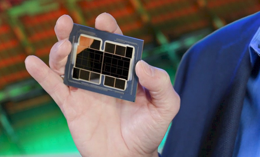
In the datacenter, “Sapphire Rapids,” the fourth generation Xeon SP due to ramp in 2022, will use the SuperFIN modification of 10 nanometer manufacturing, and “Granite Rapids” will be the first Xeon SP that uses this 7 nanometer process. Elements of the “Ponte Vecchio” GPU accelerator will also use the 7 nanometer process, and Gelsinger held it up to show it was real:
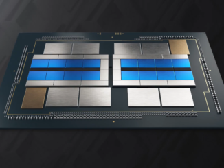
As we have previously talked about, this Ponte Vecchio device will use a mix of Intel’s EMIB 2D chiplet interconnect (which it has already used on high-end Stratix FPGAs) and its Foveros 3D chip tiling and stacking technique (which has been deployed on client Core processors). Here is an exploded view of the Ponte Vecchio package:
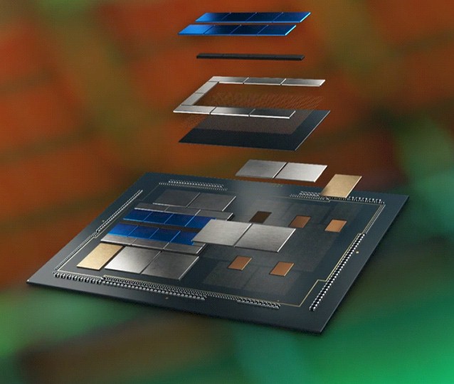
There are more than 40 different tiles, with multiple different manufacturing geometries, integrated on the Ponte Vecchio package, and some of those tiles are being made by an outside foundry, as we reported back in September 2020. The base tile in the Ponte Vecchio package will use Intel’s 10 nanometer SuperFIN manufacturing, while the GPU compute tiles will use a mix of Intel 7 nanometer and outside 7 nanometer processes. The “Rambo” cache tile for the GPU compute units will be made using 10 nanometer SuperFIN, but the Xe Link I/O tile will use an external foundry – and possibly with a fatter geometry like 14 nanometer or 16 nanometer. (We shall see.)
The Ponte Vecchio package will have more than 100 billion transistors, which cannot be put on a single chip even if we tried at 7 nanometers because it would be beyond the reticle limit of etching equipment, and even if you could make it, it would have very low yield because of its size and therefore very high cost per good die. Gelsinger called that single package “a petaflops scale AI supercomputer,” which is a shorthand way of saying it will be capable of petaops of mixed precision support and certainly less than a petaflops at double precision floating point. (Our best guess way back in November 2019, based on some pretty witchcrafty spreadsheet work to be sure, was for the Ponte Vecchio GPU to come in at 12.5 teraflops to 16.4 teraflops at double precision.) That is the main compute engine in the “Aurora A21” exascale supercomputer that Intel and HPE are building for Argonne National Laboratory, as you all well know.
This is the future for Intel, and you can bet that it wants as many of those chiplets as possible to be made in its foundries going forward. But that’s not the point of Ponte Vecchio. Flexibility and reliability is, just as is the case for the real Ponte Vecchio that crosses the Arno River in Florence, Italy, which is well over ten centuries old and which is lined with diverse shops all sharing the same bridge. This GPU accelerator package – we can’t really call it a chip – is aptly named. Perhaps with prescience, perhaps through serendipity.
From here on out, though, Intel has to execute as steadily as its rivals TSMC in foundry services and AMD in compute have done. It has to build those fabs – and more – and become a true foundry so it can afford its IDM 2.0 strategy. The time for spending $20 billion on share buybacks is done. There is a $100 billion total addressable market in foundry services (that’s year-end 2025) to chase.

The Most Complex Chip Ever Made?
Historically Intel put all its cumulative chip knowledge to work advancing Moore’s Law and applying those learnings to its future CPUs. Today, some of those advanced processors are destined for the forthcoming “Aurora” supercomputer at Argonne National Laboratory. However, demanding simulation and modeling workloads also benefit significantly from GPU acceleration. …
Programming The Network With Intel NEX Chief Nick McKeown
It would be very difficult indeed to find a better general manager for Intel’s newly constituted Network and Edge Group networking business than Nick McKeown, and Pat Gelsinger, the chief executive officer charged with turning around Intel’s foundries and its chip design business, is lucky that Intel was on an …

Who Will Build Europe’s First Exascale Supercomputer – And With What, And Why?
Exascale supercomputing is just as important to Europe as it is to the United States and China, but each of these geopolitical regions on Earth has its own way of developing architectures, funding their development and production, and figuring out where the best HPC centers are to host such machines …
I don’t believe Gelsinger cooked up this IDM 2.0 strategy. This presentation is clearly a result of all the decisions made by Bob Swan’s team in January. He’s left now, but his impact will be felt for the next few years at least.
This is a great initiative to execute. I think it helps develop manufacture.