The long-held skepticism around wafer-scale architectures is deep and goes back decades. Few have tried and all have failed, either for business or technology reasons, including the venerable Gene Amdahl. But perhaps what was missing was the right timing in equal addition to a suitably established semiconductor technology base.
If you ask Andrew Feldman why a wafer-scale approach isn’t more prevalent, his answer is simple: His team at Cerebras Systems are the only ones that has figured out how to actually do it. And in his view, no one can or will try—at least not in the near term.
“I don’t think anybody can do it. It’s taken us five years and we have a huge patent portfolio to work around. This workload, AI, will be about one-third of the total compute. If you look at Google, the canary in the compute coalmine, they’ve formed most of their work to look like AI workloads. Further, the compute being used to solve AI problems is growing exponentially, it’s astounding. Over the next three to five years, more of the work in datacenters will be AI or AI-like, more of the hard problems will be around how to find insight in that data.”
If we delicately step past that thinly veiled threat of the patent portfolio and what it mean for potential startups emboldened by the Cerebras proof of possibility, some other questions emerge. First, why didn’t this work before and second, if it’s possible now, why aren’t the majors pursuing it?
“We looked at what wafer scale was in 1984 when Amdahl did it and the truth is, that failure loomed so large in people’s memory but they never actually looked at it. Our industry was less mature, the manufacturing process around chips for sure. We’ve made hundreds of thousands of chips since then. The process and architecture are so much better. We chose an architecture for wafer scale. Gene Amdahl didn’t choose one, we tried to take an architecture he liked and bring it to wafer scale,” Feldman argues.
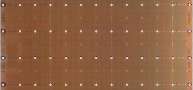
He continues, “We were able to co-design the physical reality of the chip with our architecture. One of the things we did was build a repeated tile design with over 400,000 identical blocks. That let us fail in place; if there was a failure we could route around it. The observation that was new there was how to combine the known fact that there would be flaws knowing there would be some. This isn’t new; the DRAM folks hold aside rows and columns of bit cells and they hold some aside and recruit them and that’s how they get high yields. But no one did that with compute until we did.”
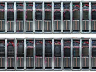
The trick might be that to do it and have a functional, efficient system, however, you can’t just sell standalone devices and not every chipmaker wants that burden (although Nvidia’s DGX machines might reflect something different). A full stack, from compiler to cooling, is the only way it can make sense. This is exactly what Feldman’s company, Cerebras Systems, is doing with its CS-1 systems. Recall that Cerebras gained some momentum with its Wafer Scale Engine approach to AI this year in particular with installations at research-centered sites, including Lawrence Livermore National Lab, Argonne National Lab, and the Pittsburgh Supercomputing Center. It’s difficult to tell where they might land in enterprise or hyperscale systems but for now, the team seems hellbent on bearing out the concept and proving that wafer-scale architectures are not only possible but functional, even outside of pure AI training and inference.
We have to assume that the massive research budgets at Intel and Nvidia have at least given the topic some thought, especially after seeing Cerebras prove the concept. Perhaps they did find ways to make all the on-chip circuitry and more important, compiler do the trick and found that while it was practical, it wouldn’t make economic sense. And just perhaps that’s because you can’t just build devices to be in 2020-2025’s wafer-scale game: the whole system has to be constructed in one of the most complicated codesign exercises known to man. Most chipmakers and accelerator startups don’t want to (or practically cannot) be in the systems business and integration of this device isn’t a typical integration process, either.
There are many opportunities for a chip that with a ton of cores that can communicate at ultra-fast speeds and those are not new. AI aside, areas in HPC, including computational fluid dynamics, which have broad commercial value (in oil and gas as one example) fit the bill, as do workloads like signal processing at massive scale. Even more nascent is the idea of switch chips, which could easily swing the wafer-scale way if it was more broadly feasible with that industry already using some of the biggest pieces of silicon already. That’s just near term. We can even take that a step further and project the idea of a system that couples a wafer scale engine linked up with silicon photonics sitting naked on a rack and able to stay cool and handle truly massive workloads without leaving the device or scaling out without all the excess heat and performance loss. But that’s for another day.
For the high-value application areas in HPC in oil and gas and supercomputing-class scientific codes, the challenge for a new architecture is always the same. The codes are largely set in stone and only recently could benefit from GPU acceleration. However, the AI story is clear for those willing to invest to a mighty degree. We’ve never been able to glean a sense of cost of the wafer-scale approach and how it differs from using the same wafer to slice and dice chips to sell individually. All the extra networking to make all the pieces connect likely comes with significant cost overhead.
For those narrowly defined application sets, will there be enough of a market to tackle to make all of this worth it? And how long will it be before one of the switch chip makers and integrators gets the cue and either buys Cerebras for its engineering and diversifies a switch chip effort with AI capability?
“If you look at Nvidia and Intel research, they were publishing papers that said it couldn’t be done. We solved a problem that’s been unsolved for 70 years. These giant companies with tens of thousands of engineers kept saying it was impossible and our small team in bad Los Altos real estate did it,” Feldman tells us. His assertion is that the big companies aren’t pursuing wafer scale because of an inherent lack of technology. “Nvidia and others knew that bigger chips were better for this workload. If you chart the size of the GPU starting in 2013 it’s more than doubled in size. Why? Because they knew bigger chips were better. But what they didn’t know how to do, still don’t know, is how to get 50 or 60 times larger—that’s what we did,” he adds.
Even if wafer-scale can and does exist, it’s not a fit for every problem by any means. But for the AI workload with its need for small, dense compute and massive communication at low power, low latency, and ultra-high bandwidth, such an approach makes sense. While other accelerators and accelerator-based systems offer this, there’s still the external network piece to get around, which is where the problem lies. Moving from a chip the size of a postage stamp to a dinner plate, however, is not easy.
But if the wafer-scale concept is proving valid, might we see other startups take a similar approach? Companies that have tight control over their own fabs could easily make the leap. While Feldman says they haven’t because they don’t know how, the reasons they don’t might be a bit more complicated and have more to do with focus, semiconductor economics, and demand. And if so, what is the potential market they would have to tackle with a product that will be anything but cheap? Considering that a company like Intel, with all the network, fab, and market know-how hasn’t gone this route, for instance, there must be something that either isn’t worth the effort or can’t be done at all.
To answer the question in the title then, is there a wafer-scale future on the horizon with at least another startup or two and perhaps one of the majors entering the game? Perhaps. This is why we’re keeping such close tabs on the machine at LLNL–not just to see if it works but how the programming model functions and if it can truly take on far more than just AI. As mentioned, it is not unreasonable to see a future with systems based on massive racks of wafers combined with silicon photonics technology that can get around the heat problem and have real communication that is partitionable, scalable, and within reasonable power budgets. Then things get interesting, especially if the magic compiler can truly work with parallel codes in HPC and large-scale analytics as well as whatever the AI workload morphs into.


It is as if Andrew Feldman has never heard of POET Technologies or their wafer-scale photonics solutions (backed up by MANY bedrock patents…)