

If you wanted to wrest control of datacenter compute as embodied mainly in the Xeon SP processor away from Intel, there are a number of approaches that you might take. You could take Intel head on in the core of its market, as AMD has done with the Epyc line of processors, pitting its designs and the chip etching might of its foundry partner – and nearly every semiconductor company’s foundry partner – Taiwan Semiconductor Manufacturing Corp against Intel’s designs and its own foundry.
Another way would be to completely change the nature of the game. This is what Marvell, a chip conglomerate founded two and a half decades ago that now has more than 5,000 employees and $2.7 billion in revenues in its fiscal 2020 ended in February, seeks to do. And rather than try to make every chip with every possible SKU that every customer might possibly need and try to get yields on that, Marvell is taking a slightly different approach. After decades of experience making storage controllers, network processors and other kinds of networking chippery and moving into Arm server processors (ThunderX), switch ASICs (XPliant and Prestera), and other devices with the acquisition of Cavium back in November 2017, Marvell has bought a bunch of assets in recent years that it is now rolling out to do mass customization of chips.
In essence, all of its intellectual property – and it has amassed a treasure trove of over 10,000 patents in the past two decades of acquisitions – and all of its skills in designing chips, packaging them up, and getting them through the non-Intel foundries to finished products. That would be TSMC, of course, but also GlobalFoundries and Samsung.
Hedging across multiple foundries is important because it is not just Intel that hits bumps when it comes to advancing process technology. GlobalFoundries hit its own wall at 7 nanometers – roughly equivalent to the 10 nanometer process that has given Intel such grief – and backed off on that more than two years ago. Samsung, which is no slouch when it comes to advanced process technology thanks to its memory and flash business and its Arm-based chips for consumer devices, is the remaining player and is also the foundry partner for IBM with Power10 and z16 server chips as it seeks to move from the edge back to the core datacenter with its skills. Marvell cannot afford to be a foundry in its own right – it does not command those kinds of volumes, given the cost of building a fab these days, well north of $10 billion – but it can position itself as an expert across the three independent foundries. And that, with the $650 million acquisition of Avera Semiconductor, the amalgam of the chip design teams from IBM Microelectronics and GlobalFoundries, is what Marvell is now starting to do. It has the portfolio of chips that customers can license and tweak and it also has the expertise to help companies do a better job getting their own chips off the whiteboard and into systems.
Marvell, which was founded in 1995 down the road from Intel in Santa Clara, has come a long way in a relatively short time to become a player in the datacenter and at the edge. During the height of the dot-com bubble, Marvell went public and raised $90 million, and its stock went so high in the fall of 2000 that it could trade $2.7 billion of that stock to buy Galileo Technology and enter the Ethernet switch and embedded controller markets.
Since that time, Marvell has included CPUs in some of its chip designs, and in 2003 it bought Asica, which was creating its own chips based on the Arm architecture and which had an architectural license with Arm Holdings, meaning it could tweak the core designs as long as it didn’t break compatibility with the Arm instruction set. Marvell designed several generations of Arm chips, used in various embedded and consumer devices, throughout the 2000s and even snapped up Intel’s XScale Arm chip business for $600 million in July 2006, which Intel inherited from the former Digital Equipment’s StrongARM line of RISC chips from the late 1990s. These two lines are the foundation of the Armada line of Arm chips, which have been used in all kinds of devices, including servers every once in a while. In July 2018, Marvell ponied up $6 billion in stock and cash to acquire Cavium, getting a slew of MIPS and Arm processor lines, including the Octeon MIPS chips used as network processors and the Thunder line that includes the ThunderX1 that Cavium itself devised mostly by swapping out the MIPS cores in the Octeons for Arm cores, and it is funny that this is essentially what chip rival Broadcom did to create the “Vulcan” Arm server chips from the NetLogic multicore MIPS chips it acquired in September 2011 for $3.7 billion. It is funny that the ThunderX2 has more in common with the NetLogic foundation than with the Octeon foundation, but also that they have similar roots.
All of this – and much more not covered here – demonstrates that Marvell has a broad and deep experience in creating chips that are suitable for the datacenter and the edge. And in fact, Igor Arsovski, chief technology officer for the ASIC business unit at Marvell, tells The Next Platform that the design team at the company, which includes people from the original Marvell plus those from Cavium, GlobalFoundries, and IBM, have brought into existence over 2,000 chips in the enterprise and networking spaces alone. (IBM Microelectronics, which has been selling custom ASICs since 1994, is a big part of that experience.) This is a very deep bench, and this is one of the reasons that AI chip startup Groq, which is unveiling its Tensor Streaming Processor (TSP100) today, partnered with Marvell to bring this chip into being.
Arsovski gave us a level set to illustrate exactly what the AI chip makers of the world are up against. Take a look:

These charts, in a nutshell, show why accelerators are necessary for any application that is both compute and memory bandwidth intensive, as machine learning training most certainly are.
“This trend of custom silicon is growing, and what is pushing it is the complexity of the models,” Arsovski explains. “The AI model complexity has actually increased by 50X in the past 18 months, and if you look at what it takes to achieve 50X transistor scaling, you are looking at about 120 months or ten years. That’s close to a 7X gap. If you look at the glory years of Dennard scaling and Moore’s Law, where we were doubling every 18 months, we have slowed down even more.”
The slowdown is especially acute when it comes to SRAM on-die memory, which is used as cache and sometimes main memory – as in many AI accelerators, for instance – in devices, says Arsovski, who is, as it turns out, an expert in designing SRAM who hails from IBM. If you stay on the advanced process nodes, it takes around five years to double the amount of SRAM per square millimeter. Almost all of the AI accelerators that are not based on GPU designs have giant blocks of SRAM as well as matrix and vector math units next to them or they might have high bandwidth memory of some sort as well, either now or in their future. The FPGA AI accelerator designs that are based on overlays of what are in essence virtual compute engines use block RAM (BRAM) implemented in logic right next to the compute in much the same way. The point is, get enough high speed memory on the device itself so the models can fit on the device and training or inference can be done within that memory space without resorting to external memory.
That works for now, and maybe even at the 7 nanometer or 5 nanometer nodes. We think that given what Arsovski says above, and the slowdown in Moore’s Law in general, everyone will be looking at some sort of GDDR or HBM or HMC memory to wrap around their future AI compute devices because there is no way to have the SRAM scale at the same pace as the compute on any device, regardless of node.
In fact, we think there is a very good chance that compute will stay on a higher yield part of a multichip module and SRAM memory will be etched using the most advanced nodes, but that assumes there can be very low latency and very high bandwidth connectivity between the two. As Arsovski reminds us, and which we know full well, going to memories off any die, the bandwidth drops by about two orders of magnitude. Having said that, Marvell has worked with Micron Technology to integrate its Hybrid Memory Cube memory with TSVs to compute in a 3D stacked package. This one possible path for AI accelerator design when the SRAM density starts running out of gas.
There is a reason why Groq picked Marvell as its design partner for its TSP accelerators, and SRAM was a big part of that reason, according to Arsovski. Groq wanted to use a mature 14 nanometer or 16 nanometer process to increase yields and to lower risk on its first chip, and with the experience that IBM had with designing its Power9 server CPU for the 14 nanometer processes at GlobalFoundries, this was a good fit, given that it has 220 MB of SRAM across the chip:
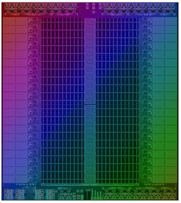
That TSP 100 die weighs in at over 700 square millimeters in area, and as you can see, it is dominated by huge SRAM blocks in the center. There is an east and west bank, each with 44 independent banks, and the combined bandwidth across that SRAM is a stunning 27.5 TB/sec. The HBM2 bandwidth on the Nvidia “Ampere” A100 GPU accelerator is 1.55 TB/sec, and the latency between that memory and the cores on the GPU is, as Arsovski points out, orders of magnitude larger than the on-die SRAM latency.
Arsovski brags that the SRAM that Marvell can bring to bear for Groq, thanks to the Avera acquisition, is 10 percent to 15 percent denser – at 11 megabits per millimeter square – than what was possible from other designers using 14 nanometer or equivalent 16 nanometer technology. And that SRAM in the Groq TSP 100 is two ports running at 1.2 GHz, so it will have twice the bandwidth of a single port SRAM implementation, and thus the bandwidth is a lot larger than what might have been done with other designs.
The partnership between Marvell and Groq was not just about SRAM. Marvell had high speed SerDes it could donate to the cause as well as full turnkey PCI-Express and chip-to-chip interconnect (C2) subsystems that Groq could leverage, and most importantly, Marvell has the expertise to deliver chips that yield well and work in the field – experience that Groq itself does not have and, if this partnership works into the future, will never have. Here’s the neat bit. The Groq TSP 100 went from final netlist – the flow chart of connectivity between components in a circuit design – to tape out in under three months thanks to the expertise at Marvell. Time to market is going to be critical for any mass customization effort, particularly when products won’t be high volume or long lived as we think they won’t be in the future.
Hardware will be more like software, which has always been the dream, of course. And that does not necessarily mean because of programmable logic. We believe that compute engines are going to get more expensive at a socket level over time because they will have to include chiplet architectures and they will sometimes deploy reticle-busting approaches thanks to the slowdown of Moore’s Law. And because compute engines will be tuned very specifically for workloads, they will by necessity be etched in smaller runs and packaged up as they come out of the foundries, which also increases their cost. But, but, but we also believe there will be very little dark silicon and they will run at high utilization, and therefore the actual price/performance of the devices will still follow something that roughly approximates a Moore’s Law curve. And fast iteration of compute engines, using all the available tools and technologies, is what is going to keep progress happening. Those who can’t iterate fast and find and keep customers moving are going to be left behind.
That is what Marvell is betting on, and indeed also what Intel and TSMC and GlobalFoundries and Samsung are betting on, too.
Mixing And Matching Foundries
People forget sometimes that not every device in the world needs to be on the most advanced node. To be fair, many of the coolest devices – pun intended – are on the tiniest transistors, but it is not a prerequisite in a world where price/performance matters most and co-designing hardware and software allows for every transistor to be doing something useful for a specific workload.
To get a better handle on the mass customization business that Marvell has wrapped up for chip designers, which puts its entire portfolio of intellectual property as well as its hardware engineers at their disposal, we had a chat with Kevin O’Buckley, general manager of the ASIC Business Unit and like Arsovski, a long-time IBMer who did a stint at GlobalFoundries after Big Blue sold its chip business to the former AMD chip foundry. O’Buckley rose through the ranks at IBM Microelectronics, working on its copper and SOI processes during the dot-com boom and bust eras and then heading up the development of the Cell hybrid CPU-GPU processor used in game consoles and supercomputers at the 90 nanometer and 65 nanometer nodes in the 2000s. O’Buckley eventually was responsible for developing the 22 nanometer and 14 nanometer processes at IBM Microelectronics, which GlobalFoundries took over when it bought this IBM unit, and then managed a team of more than 1,000 engineers that were working on 14 nanometer, 12 nanometer, and 7 nanometer processes at GlobalFoundries.
If anyone understands the dependence of chip designers on foundries – and who wants to break that dependence to de-risk the task of bringing chips to market – it is O’Buckley. And that is why Marvell has assembled a team of people who understand the GlobalFoundries 22 nanometer, 14 nanometer, and 12 nanometer processes, the TSMC 7 nanometer and 5 nanometer processes. And we would not be surprised to see some expertise in Samsung’s 7 nanometer and 5 nanometer processes emerge as well. Until Intel gets its foundry act together, we don’t expect much cooperation here, and if anything, it would be interesting to see Intel try to buy Marvell. (But that is a crazy idea for another day. . . . )
As we pointed out above, Marvell has amassed a huge portfolio of circuits, which this image captures nicely:

The one thing that Marvell doesn’t own is an FPGA. It could buy one of the upstarts, such as Achronix or Lattice Semiconductor, to fully flesh out its portfolio, but it seems far more likely that it can just partner with these two and Xilinx as well to bring FPGA functionality into its stack. O’Buckley said Marvell is in fact talking to customers about custom chips that include FPGA elements and added that, like us, he believes there will be more emphasis on FPGAs in the future because software and hardware will have to be tightly tuned in many ways and ASICs are not always the answer.
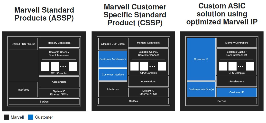
Now that Marvell has bought Avera as well as Aquantia, which it also bought last year to flesh out its automotive networking capabilities, here is the customization spectrum that it can offer to customers, ranging from standard products fully designed by Marvell, like its Octeon or ThunderX chips, to semi-custom chips that include homegrown as well as Marvell IP:
This customization is not for everybody today, and Marvell knows that. “From a revenue standpoint, maybe 20 percent or more of the market will require some kind of custom silicon,” O’Buckley tells us when pushed for a hunch number. “The majority of the purchase of semiconductors in the industry will continue to be buying standard products. And that is really a question of scale and money. Even at the slightest level of customization, you are investing millions of dollars into those products.”
To give an example, IBM had more than 100 engineers working on the customization of Cell processors for game consoles. This is not cheap, but Microsoft, Sony, and Nintendo got exactly and precisely what they needed from IBM, just as they are getting from AMD today. And maybe Marvell in the future.
It is interesting that Marvell is taking some of its own semi-custom medicine. With the “Triton” ThunderX3 processor, which we did a deep dive into as part of our Hot Chips coverage in August, Marvell is not going to be doing a full SKU stack and big launch. Rather, given that a market of broader enterprise users of Arm processors has not yet materialized and its relatively few (in terms of number, not in spending) hyperscaler, cloud builder, and HPC customers want unique customizations, Marvell is instead going to treat the ThunderX3 as a semi-custom chip and sell it directly through engagements. But don’t get the wrong idea. Marvell absolutely believes that there will be a broader Arm server chip market in the future – it is just not here today.
And maybe, just maybe, the future of server compute will resemble the custom game console chip business when it does arrive than it does the Intel Xeon SP server chip business of today. That’s our bet. And in that world, it makes a whole lot of sense for Nvidia to be buying Arm Holdings, among other tectonic shifts we will undoubtedly see.

The Road Ahead For Datacenter Compute Engines: The CPUs
Updated with just-announced Intel roadmap changes. It is often said that companies – particularly large companies with enormous IT budgets – do not buy products, they buy roadmaps. No one wants to go to the trouble of optimizing software for something that turns out to be a one-off product, forcing …
Red Hat Woos VMware Shops With OpenShift Virtualization Engine
Broadcom’s $61 billion acquisition of VMware in November 2023 and the subsequent changes to venerable virtualization company’s business model and pricing have rankled many long-time enterprise users, a situation that has been highly publicized despite assertions by Broadcom and VMware executives that such reports are little than FUD – short …
IBM Takes The Patient Path To Future GenAI Profits
While the hyperscalers and cloud builders provide the best indicator of what it takes to create state of the art GenAI models and the infrastructure to train them as well as to put them into production for practical use through an API interface, perhaps IBM is one of the best …
Be the first to comment