

Ayar Labs looks like it is just about ready to put its optical I/O chiplet technology into commercial datacenter products. A presentation at the recent Hot Chips conference revealed a lot more detail about Ayar’s technology than it has have offered in the past, while also divulging that it is now working closely with a prominent chip vendor. Named Intel.
That revelation was given out by Mark Wade, the company’s chief scientist, president, and co-founder. But before we get to the Intel part of the story, it is important to describe what led up to it. And from Wade’s perspective, Ayar’s story began with the idea of solving a persistent problem that faces the entire computer industry.
“Our motivation is simple,” Wade explained. “We believe that long-range electrical SerDes does not have a roadmap beyond 112 Gb/sec signaling. So this opens up a huge need for the industry to come up with a new general-purpose universal I/O technology to supply high-bandwidth I/O to and from high performance SoCs.” This is not a belief held just by Wade alone, but by most luminaries in the industry, including none other than Andy Bechtolsheim, who was talking about the 100 Gb/sec – that’s the effective bandwidth after encoding overhead is taken out – signaling wall early last year.
That need is currently not being met because commercially available optical I/O devices currently only exist for communication that is outside the server box, that is, for local and wide area networks. For the shorter distances involved for in-package and on-board communication, electrical-based communication is still king. In-package communication, such as that provided by high-bandwidth-memory (HBM), is the most capable, providing lots of bandwidth at relatively low power consumption. By contrast, on-board communications, like PCI-Express and NVLink, deliver about one-tenth the bandwidth of in-package solutions and are proportionally less energy efficient.
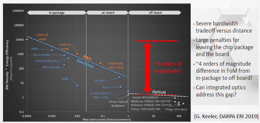
But as Wade notes, the big gap comes with optical, which supports communication across much longer distance – from multiple meters up to multiple kilometers. Unfortunately, the density and energy efficiency of those solutions precludes it from being inside the computer. Using the figure of merit of bandwidth density * energy efficiency, Wade explained that there are about four orders of magnitude difference between current optical solutions and electrical ones.
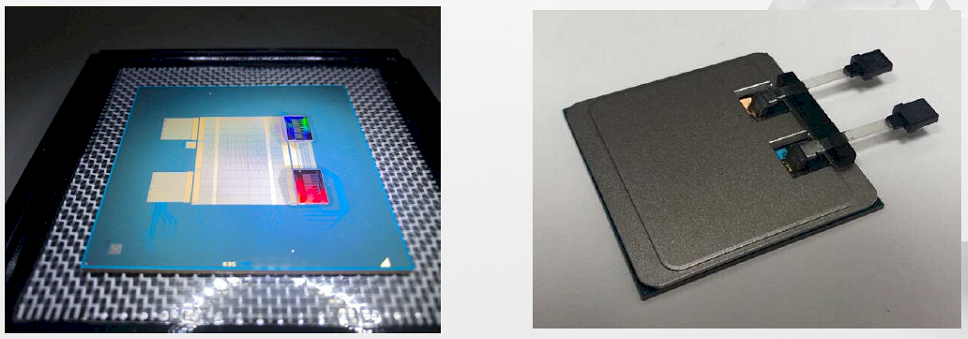
And that’s what his company aims to solve with its TeraPHY chip – or more precisely, chiplet. As we explained when we first covered Ayar Labs in January, the TeraPHY is an optical transceiver that is designed to provide I/O communications for the other chiplets on the package, whether they be CPUs, GPUs, FPGAs, or ASICs. Essentially, Ayar engineers figured out a way to etch optical devices onto on conventional CMOS, which is key to closing the density and energy efficiency gap between electrical short-distance I/O and long-haul optical.
The basic building block for the TeraPHY chiplet is something called a microring resonator, a type of optical circuit that acts similarly to the Mach-Zehnder Interferometer (MZI) used in long-distance optical devices. Except the microring is 100 times smaller, has 25 to 50 times the bandwidth density, and about 50 times the energy efficiency of an MZI. At a size of 10 micrometers, a resonator is able to deliver 25 to 100 Gbps.
The other ingredient in Ayar’s secret sauce is something called a vertical grating coupler, which acts as a phased-array antenna to scatter the light and pass it to the optical fiber. Essentially, this is what enables light to be funneled on and off the TeraPHY chiplet.
The light source, a “SuperNova” laser, is provided as an external device that feeds photons into the TeraPHY chiplet. Wade said the decision to keep the laser as a discrete component, rather than integrating it on-chip was to simplify the packaging and let the laser and the transceiver evolve on their separate paths. And since this laser will presumably sit somewhere on the board, it won’t impact communication latency appreciably.
By cascading these microring resonators along the same waveguide, the TeraPHY is able to support a wave division multiplexing, enabling the chiplet to use multiple wavelengths of light from the laser. That means you can send and receive a lot more data on a single optical fiber. This will allow them to scale the architecture to as many as 64 wavelengths once the laser technology catches up.
The TeraPHY is divided into transmitter and receiver components, which are symmetrical with 10 TX/RX macros. Each part will support between 1.28 and 2.56 Tbps, depending upon the optical modulation rate. All of this on a die that is 8.86 millimeters by 5.5 millimeters using GlobalFoundries’s 45 nanometer process. According to Wade, the whole thing operates at less than 5 picoJoules (pJ) per bit.*
Note that the energy efficiency number takes into account the electrical components on the chiplet as well. This circuitry is used on the backend of the transmitter and receiver so that, as Wade put it, “we can mostly make our chip look like an electrical chip.” TeraPHY also has additional electrical components that are used for things like clocking, drivers, amplifiers, and other control circuitry.
So how does this turn into something usable? That’s where Intel comes in. Ayar has been collaborating with the chipmaker on what amounts to a proof-of-concept SoC package that includes two TeraPHY chiplets and a Stratix 10 FPGA. Ayar are using Intel’s Embedded Multi-Die Interconnect Bridge (EMIB) 2.5D package technology, which enables multiple chiplets to be laid across a common silicon bridge. The device also uses the Advanced Interface Bus (AIB), an open-source standard developed at Intel, which the chipmaker hopes will be adopted by other vendors.
Supposedly Ayar chose EMIB and AIB for a number of technical reasons. EMIB offers mixed bump pitches for the same die and dense die-to-die connectivity, while AIB was appealing due to its simplicity, energy efficiency, low latency, and compelling roadmap. But the collaboration may turn into a full-fledged commercial partnership if Intel decides to use TeraPHY in its upcoming AgileX FPGA products, which will also employ EMIB and AIB technology.
At present, Intel is saying those products will use 112 Gb/sec transceivers, presumably driven electronically, but that wouldn’t prevent them from adding an optical transceiver option at some point. And perhaps Intel even has designs on the Ayar chiplets for its future Foveros 3D system-in-package platform.
Wade didn’t offer any speculations such a partnership. His main thrust was that on-package optical could end up filling the roll of a universal I/O platform, enabling the same hardware to be used for communication between sockets or systems, spanning everything from centimeters to kilometers.
“The promise of optics is you have almost fundamentally broken that distance sensitivity whenever you try to increase bandwidth,” he argued. “So the traditional bandwidth-density tradeoff all but disappears in how systems are architected today.”
[*Editor’s note: paragraph has been updated to reflect latest specifications.]

With Gaudi 3, Intel Can Sell AI Accelerators To The PyTorch Masses
We have said it before, and we will say it again right here: If you can make a matrix math engine that runs the PyTorch framework and the Llama large language model, both of which are open source and both of which come out of Meta Platforms and both of …

AI At The Edge Is Different From AI In The Datacenter
Today’s pace of business requires companies to find faster ways to serve customers, gather actionable insights, increase operational efficiency, and reduce costs. Edge-to-cloud solutions running AI workloads at the edge help address this demand. Placing compute power at the network edge, close to the data creation point, makes a vital …
Intel’s Datacenter Business Goes From Bad To Worse, With Worst Still To Come
Everybody expected that Intel was going to turn in a pretty bad final quarter in 2022, and even before it posted its numbers yesterday after the market closed, there were plenty of signals that it was going to be worse. And it was. And the worst is still yet to …
After viewing the slides from Hot Chips, I would guess the next step would be to have an optical/copper PCB and and do away with the flyover optical cables.