
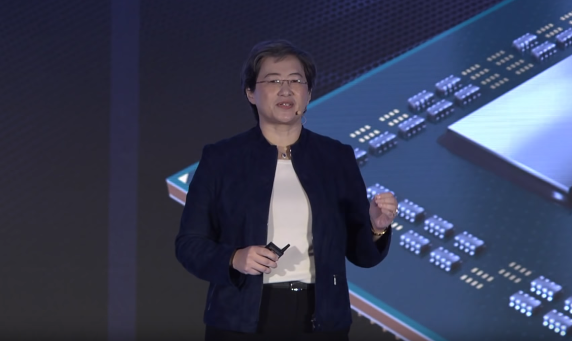
It was a long time coming but AMD is finding its footing again in the high performance computing space. At the Computex tradeshow this week in Taipei, CEO Lisa Su talked about her company’s Epyc processors and how they are fulfilling the chipmaker’s HPC ambitions.
The Computex event is heavily skewed toward personal computing gadgetry, so most of the chatter there is about laptops, gaming platforms, smartphones, and the like. Even so, Su spent about 10 minutes of her conference keynote address on their Epyc silicon and almost all of the presentation was devoted to how the architecture has delivered some key successes in HPC on a number of different fronts.
One of those is the company’s huge Department of Energy win for the upcoming “Frontier” supercomputer at Oak Ridge National Lab, which Su recapped during her opening talk. The Cray-built machine, which is scheduled to be installed in 2021 or 2022, will be powered by future custom-built Epyc CPUs and Radeon GPUs, delivering 1.5 exaflops. Having bested both Intel and Nvidia in the competition, the deal gives AMD newfound credibility at the upper echelons of supercomputing.
Su also used her Computex address to reveal that Epyc processors are being used to break new ground in cloud-based HPC. Specifically, Azure HB-series virtual machines were used to scale a computational fluid dynamics (CFD) code to 11,250 cores, using Siemens’s Star-CCM+. The HB series, which are equipped with Epyc 7551 CPUs and 100 Gb/sec EDR InfiniBand, was launched last year by Microsoft to provide an Azure offering for HPC codes hungry for memory-bandwidth. That’s aimed at applications like fluid dynamics, explicit finite element analysis, and weather modeling, among others.
According to Microsoft, the 10,000-plus-core run represents the first time an MPI-based HPC application achieved that level of scalability in a public cloud. And apparently, that’s not the upper limit. A single distributed memory job can use up to 18,000 cores and more than 67 terabytes of memory with Azure’s HB VMs. Here is the raw data for the runs that Microsoft did:
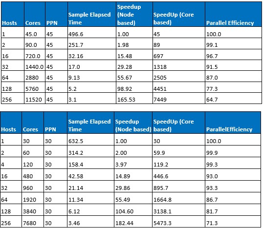
And here is the graphical representation showing the scaling on Star-CCM against ideal scaling for different levels of granularity in the code:
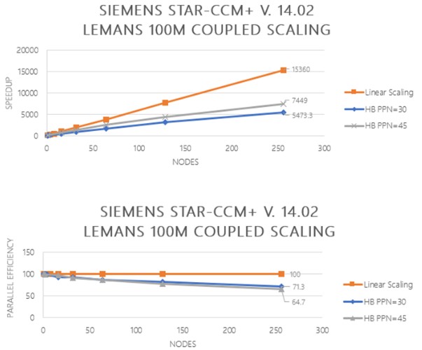
“The idea here is that we have the ability to have the largest cluster of Epyc CPUs that will really allow you to simulate very, very large tasks,” said Su.” Our first customer has already said that they have been able to get a 7,500 speedup by using the Azure cloud with Epyc compared to what they could do before.” The CEO also noted the Baidu and Tencent have brought Epyc processors into their respective clouds.
AMD’s second-generation Epyc, codenamed “Rome,” should be able to accelerate the company’s HPC momentum even further. Having successfully leap-frogged over Intel’s 14 nanometer manufacturing technology, the new 7 nanometer Epyc chips will sport up to 64 cores, double the number in the original Epyc. The vector units in the Rome designs are twice as wide, too, and so as a consequence, Rome will deliver 4X the raw floating point performance of the first-generation “Naples” Epyc processors. That last bit is critical, since the original chips, while superior in memory bandwidth compared to their Xeon counterparts, did not have the same level of floating point math performance.
To illustrate that point for the Computex crowd, AMD datacenter general manager Forrest Norrod came onstage to show how fast the Rome processors were compared to Intel’s latest Cascade Lake Xeon processors. Using NAMD, a molecular dynamics code, a dual-socket server equipped with Rome processors outperformed a dual-socket server equipped with 28-core Xeon 8280s by a factor of two, racking up twice the simulation time for a High Density Lipoprotein (HDL) molecule. Norrod mentioned that that the Xeon 8280 lists at $10,000, implying that their top-end chips will be priced below that.*

It would have been interesting to pit the 64-core Rome against a 56-core Xeon 9282, the top-of-the-line Cascade Lake AP processor, which is said to deliver twice the performance of its 28-core sibling. Intel isn’t disclosing pricing on the Cascade Lake AP chips since they are only being sold to server manufacturers in the form of Intel-designed systems with Intel motherboards. That and the fact that they draw 350 watts to 400 watts puts them in a somewhat different category, server-wise.
Although Su didn’t mention it, Rome has already nailed a couple of big wins for HPC supercomputers that will be deployed in Europe. One is a 24 petaflops system built by Hewlett Packard Enterprise for the High-Performance Computing Center (HLRS) of the University of Stuttgart, which is scheduled to be up and running by the end of the year. The other is a 6.4 petaflops BullSequana machine, which was purchased by the Finnish IT Center for Science. It’s scheduled to be installed in 2020.
With all these Epyc success stories under its belt, HPC now appears to be a central pillar of AMD’s datacenter strategy. “We believe that supercomputing is at the forefront of computer architecture and the innovations in technology that’s driven into systems wind up defining the standard for the datacenter,” Norrod remarked, in a company video on the subject.
Whether that’s true or not is debatable, but success in the HPC arena does confer a certain legitimacy to play in other datacenter environments. In fact, before Intel became more enamored with other application areas like AI and hyperscale computing, HPC was driving their server processor architecture as well. In any case, we will see if AMD’s strategy continues to pay dividends as Rome hits the streets in the third quarter of the year.
*Intel is disputing the results of the NAMD test, claiming that the proper optimizations were not used for the Xeon server test run. When they supply us with the specifics, we will update the article with that information.

Datacenter Will Be AMD’s Largest – And Most Profitable – Business
Two and a half years into the global coronavirus pandemic we all have upgraded our home IT infrastructure. And after several fibrillatory interest rate shocks by the major governments to try to curb inflation in the world economy, spending on PCs has consequently taken a nose dive. And a glut …

High Performance Computing Will Power The Next Normal
High Performance Computing is traditionally focused on solving the most complex problems in science, engineering, and business. Weather forecasting, for example, takes enormous computing capabilities. As compute advances, so does the accuracy of the forecasts. With the emergence of the COVID-19 pandemic, the need for HPC became even greater and …
AI Hype Will Drive Datacenter GPU Prices Sky High
UPDATED Like many HPC and AI system builders, we are impatient to see what the “Antares” Instinct MI300A hybrid CPU-GPU system on chip from AMD might look like in terms of performance and price. And with the ISC 2023 supercomputing conference coming up in a few weeks, and Bronis de …
It appears there is a minor typo. The Hawk machine at HLRS will have 24 petaflops instead of the 2.4 petaflops in the article 🙂
And needs to ASAP get its entire line of Vega-2 GPU micro-architecture based(Vega 20 or any new Vega-2 micro-architecture based GPU base die tapeout) SKUs ready. And currently AMD’s Radeon Pro V340 datacenter graphics card is based on dual Vega 10 GPU DIEs on a single PCIe card with each of the 2 Vega 10 DIEs binned down to a similar number of Shader cores, TMUs, and ROPs as the consumer Vega 56 Vega 10 variant at 14nm.
So AMD has that single Vega 20 GPU base die tapeout at 7nm that’s currently used for Radeon Instinct(MI50 and MI60) and Radeon VII(Consumer binned variant of Vega 20, Less FP 64 enabled 1/4 ratio instead of 1/2 ratio and less Shader cores enabled, etc.). And the Radeon Pro V340 Dual Vega 10 GPU Die variant needs to be updated with 2 Vega 20 GPU DIEs and maybe at 7nm AMD can make use of all of the 2, Vega 20 DIEs’ full complement of shader cores, TMUs, and ROPs as well as all the extra DP FP units on the Vega 20 Die/Tapeout compared to Vega 10 Die/Tapeout and still make the thermal budget to allow for a passively cooled dual GPU/Single PCIe card server graphics card(Cloud game streaming/etc.) usage model. And and V340 replacement should be wired up via xGMI across the PCIe card’s PCB and not use PCIe for the GPU die to GPU die interfacing as was the method used on the older Dual GPU Die/single PCIe card professional variants.
Vega 20(Vega-2 GPU micro-arch) with its new AI focused ISA extensions has to date not seen enough attention focused on those AI oriented ISA extensions and Vega 20 is really AMD’s compute/AI oriented/focused line as opposed to the upcoming Navi based offerings that appear to be targeted more towards consumer gaming with less emphasis on any extra on GPU Die FP 64 units or excessive shader core counts.
And Now AI even has its graphics oriented usage model via AI based image de-noising/anti-aliasing, as well as AI based Photoshop filter effects, so any Vega 20/Vega-2 micro-architecture update for that Radeon Pro V340 will be of use for Google’s Stadia and other’s Cloud game streaming or visualization workloads, pro workstation graphics workloads also.
AMD needs to complete that 7nm Vega-2 transition for it’s professional Radeon Pro WX line of Pro Graphics Workstation GPUs also to be more competitive with Nvidia’s Professional RTX Quadro graphics workstation GPU offerings.
And AMD really needs to move towards more integration of Epyc/Rome and its Vega-2 and Navi(If there are any professional variants in the pipeline based on the Navi GPU micro-architecture) professional GPU offerings and that includes any Epyc CPU to Radeon GPU xGMI(Infinity Fabric) direct attached GPU accelerator interfacing that’s similar to Nvidia’s NVLink 2.0 based GPU to Power9 direct attached Nvidia GPU accelerator usage model.
I’m sure that AMD’s AI/Compute focused GPU offerings will be using xGMI(IF Based) links to communicate more directly with whatever that custom Epyc CPU variant that AMD is creating for the DOE’s AMD/Cray 1.5 exaflop supercomputer. But what about the regular server market and regular Epyc/Rome or Epyc/Milan and xGMI based Epyc CPU to Radeon GPU accelerator offerings. AMD’s been including xGMI IP on its CPUs since its Epyc/Naples offerings where released but that’s been more used for inter-socket Epyc CPU to Epyc CPU interfacing via the Infinity Fabric protocol.
So will that xGMI Epyc CPU to Radeon GPU usage model become available with Epyc/Rome or Epyc/Milan(Zen 3 CPU Micro-Arch) offerings. The Infinity Fabric is definitely AMD’s IP competition against Nvidia/NVLink(2.0) as the current Radeon Instinct MI50/MI60 variants make use of xGMI/IF Protocol via a physical bridge connector that can wire up to 4 Radeon Instinct MI50’s or MI60s into more of a single larger logical GPU in a similar manner to what NVLink is used for By Nvidia for its Tesla(Compute) and Quadro(Pro Graphics) GPU offerings.
Let’s hope that by the time that the Hot Chips 2019 Symposium is over that there will be more Known about Epyc CPU to Radeon GPU xGMI based interfacing on
Epyc/Rome, or will that have to wait for Epyc/Milan. Nvidia and OpenPower are certainly not standing still nor will Intel be after sometime in 2020-2021 as far as discrete GPUs, FPGA also, based Compute/AI accelerators are concerned from Intel.
AMD and Xilinx may have to intensely cohabitate with each other sans any nuptials exchanged if Intel keeps moving forward with its in-house designed FPGA products! And that’s in addition to Intel’s future entry into the discrete GPU market place(Professional and Consumer discrete GPUs). Ditto for Nvidia and IBM/OpenPower and some FPGA IP(partner or in-house FPGA IP) arrangement.