

Another Hot Chips conference has ended with yet another deep learning architecture to consider. This one is actually quite a bit different in that it relies on analog computation inside flash memory for inference.
Mythic, which was founded in 2012 by Dave Fick (also CTO) and a colleague from the Michigan Integrated Circuits lab has managed to raise $55 million from a number of investors, including SoftBank for its ultra low-power approach to inference at the edge. What is unique here is not just the hardware approach but also that the inference chip puts server class silicon to the test in terms of capability and certainly power consumption.
This week at Hot Chips we already talked about some different ways of thinking about MAC engines (including via Arm’s new machine learning processor) but Mythic takes the same ideas about trimming down MAC operation overhead and turns it on its head. Instead of reusing the weights (the highest overhead due to accesses versus computation) or reducing the weights by precision or compression, Mythic skips much of the MAC hit entirely. For most of you, that probably requires a denser explanation.
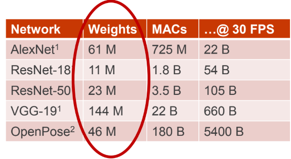
Neural networks are largely MAC (multiply-accumulate) based. There can be millions of these operations in a typical neural network and while they are not complicated at all, the real question is how many picojoules one needs to execute one of these operations. Getting the data to this unit is the hard part. The weight data for the neurons (or trained parameters) and the intermediate data (the input and output vectors) change each cycle and have different properties.
The size of the weight matrix is thus far larger than other accesses for things like intermediate data accesses. And while it has been tried, storing the data all in DRAM to make this more efficient isn’t the answer since yes, it is possible to fit large models but that comes with a cost for reading weights and provides limited bandwidth to get to the weight data. There are also other strategies to get around these inherent inefficiencies in terms of reusing weights, but that doesn’t work well with small batch sizes and compression or weight precision loss comes with capability limitations.
That was a long way of explaining how Mythic came to non-volatile memory and removing the weight of the weights almost entirely (again, for edge inference).
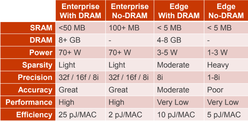
Take a look below at these common neural net accelerator design points for enterprise and edge. The latter must be small and lower power. On the DRAM versus non-DRAM side is the question of fitting the entire application on chip or not; it’s no big deal for server side work but for edge it’s not possible to add that and make use of sparsity and compression. This is a baseline.
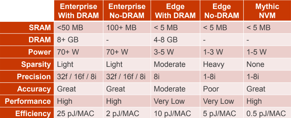
So mythic introduces a new type of non-volatile new memory that fits an entire application on a chip with a smaller power budget that is on par with enterprise chips and with quite good reported performance.
Interestingly, Mythic says it is “resetting Moore’s Law” which is a slick way of saying they’re doing this at 40nm for reasons that we are sure are more nuanced than allowing improvements at 28nm versus pushing the 5 and under envelope.
At a lower level, this idea of matrix multiplication memory without reading weights and only paying for MAC is done with analog circuits—flash transistors that can be modeled as variable resistors representing the weights. This ultimately allows for those “free” accesses and also eliminates the need for large batch sizes, sparsity or compression or “nerfed” DNN models.
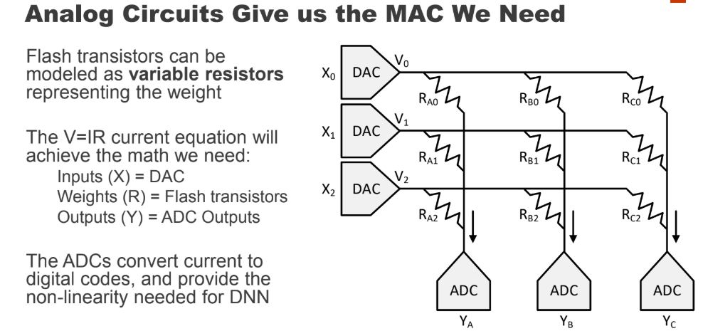
In the variable resistor array above each is a flash transistor that can be programmed and read again for accuracy. Instead of trying to read individual cells, Mythic applies a set of voltages to the input vector and gets a set of currents as outputs that are then run through the ADCs to turn those currents into values.
In other words, the flash transistors will generate current currents and those will summon the bitline and the resulting formal current represents the answer to the question being asked. Mythic uses a digital approximation technique for input.
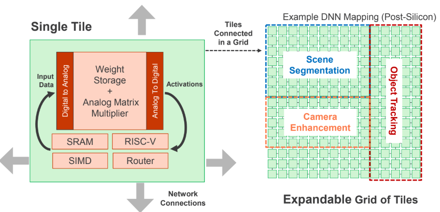
Above you can see how Mythic can take the above array (the pink middle box) and pack this into tiles with one memory array and other logic that supports configuration and intermediate data storage (the SRAM) with a RISC-V control CPU, router, and the SIMD unit for matrix multiples. It is shown here in a camera for on the fly AI.
The initial system can have a 50 million weight capacity and currently is designed with four lanes of PCIe. Fick says they can also make variants with up to 250 million weight capacity, 16 lanes of PCIe or USB as well as the use of an enhanced control processor (ARM for instance).
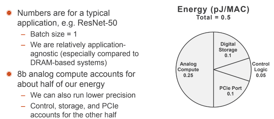
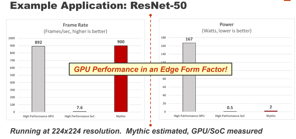
The full accounting of energy consumption is below. This is for everything—the digital logic, I/O, PCIe, etc., the entire process. It is followed by their ResNet results on what we assume to be a Tegra GPU.
The first generation release of software tools and the profiler will be available late this year. PCIe development boards with 1 and 4 IPUs will arrive mid 2019 with volume shipments of both chips and PCIe boards with 1,4 and 16 IPUs expected.

AI Powerhouses Choose The Nuclear Option
When you need to provide electricity to power and cool 100,000 accelerators, or maybe even 1 million of them in a few years, in a single location to run an AI model, you have to start thinking about the unthinkable if you also want to use carbon-free juice to power …
Nvidia Rolls Out Blueprints For The Next Wave Of Generative AI
Hardware is always the star of Nvidia’s GPU Technology Conference, and this year we got previews of “Blackwell” datacenter GPUs, the cornerstone of a 2025 platform that includes “Grace” CPUs, the NVLink Switch 5 chip, the Bluefield-3 DPU, and other components, all of which Nvidia is talking about again this …
The Balancing Act Of HPE’s Systems Business
There is perhaps no better logo for Hewlett Packard Enterprise than the box. HPE receives a bazillion boxes of components, assembles them into boxes we call servers, storage arrays, and switches, and then ships them out wrapped in other boxes to its millions of customers worldwide – mostly, by volume, …
Be the first to comment