
The world would be a simpler place for all processing engine makers if they just had to make one device to cover all use cases, thus maximizing volumes and minimizing per unit costs. Even in a world dominated by X86 general purpose compute, the SKU stacks still got pretty hairy, and by comparison, even the ever-widening “Ampere” GPU accelerator product line from Nvidia is still relatively simple.
But, to attract different customers, it still takes optimizations of price, thermals, and performance. Nvidia has pulled these levers in a slightly different way to come up with an inference engine variant of its “Ampere” GA107 GPU, called the A2 and etched in 8 nanometer processes from foundry partner Samsung. It is better suited to hyperscale and cloud datacenters with modest machine learning inference workloads as well as edge computing workloads where low power, low cost, and reasonable performance are all imperative.
We focus on the Nvidia compute engines suitable for datacenter and edge uses here at The Next Platform, and that has meant the GA100 variant of the Ampere architecture used in the big, bad A100 accelerator launched in May 2020 as well as the A30 accelerator that came out in April 2021. The GA100 is designed specifically for dense datacenter compute – the kind that drives HPC simulation and modeling as well as AI training workloads. The GA102 GPU, which was predominantly aimed at gaming uses, also supports inference and visualization (thanks to RT ray tracing cores), and is deployed in the Nvidia A10, A40, and A6000 accelerators. We did a deep dive on the GA102 and its accelerators and graphics card uses in October 2020.
The Nvidia A2 accelerator announced during the GTC 2021 fall conference last week actually makes use of a very cut-down GA107 GPU, which has not been used in datacenter or edge use cases thus far. Some of Nvidia’s customers apparently wanted a part that fit in a much smaller thermal envelope yet still had a decent price and acceptable performance for inference – hence the A2. The full-on GA107 has 24 streaming multiprocessors (SMs), which are akin to a core on a CPU; across that complex the GA107 chip has 24 RT cores for ray tracing, 96 Tensor Cores for matrix math, 3,072 FP16 units, 1,536 FP32 units, and a mere 64 FP64 units. The GA107 is used in the RTX 3050, RTX 3050 Mobile, RTX 3050 Ti Mobile, and RTX A4 Mobile graphics cards, as well as in the A16 professional graphics card, which packs four geared-down GA107s on a single PCI-Express x16 card rated at 250 watts.
The A2 accelerator optimizes the Ampere design for a small form factor and for cost per watt per unit of inference performance, which are important for in-server inference acceleration in the datacenter and at the edge. While lots of CPUs are getting pretty respectable inference performance as vector engines are sliced up into mixed precision units and as matrix engines are added to the architecture – IBM’s “Cirrus” Power10 chip and Intel’s “Sapphire Rapids” Xeon SP processor both have native matrix math engines on them – none of these speak CUDA and it takes some effort to move inference algorithms from CUDA to other architectures like Intel Xeon SPs or IBM Power. With the A2 accelerator, customers can train AI on clusters with big fat nodes housing many of the A100 accelerators and then run their inference on the much cheaper A2 accelerators in production servers. The GA107 GPU was never great at the 64-bit FP64 processing that many AI training and HPC simulation and modeling workloads need, and the cut down GA107 GPU used in the A2 accelerator is really bad at FP64 math – and so by design, given its use case.
To be precise, the GA107 used in the A2 accelerator has only 10 of its 24 SMs, 10 of its 40 Tensor Cores, and 48 of its 96 RT cores fired up. Its peak power draw drops from 250 watts to 60 watts, and then customers can customize it with software tuning to run as low as 40 watts – with a consequent further lowering of performance, of course.
Here is a table that shows the feeds and speeds of the prior generation of Nvidia “Volta” GV100 and “Turing” TU104 GPUs that were used for datacenter compute compared to the three Ampere GPUs – GA100, GA102, and GA107 – that Nvidia puts into datacenter and edge products:
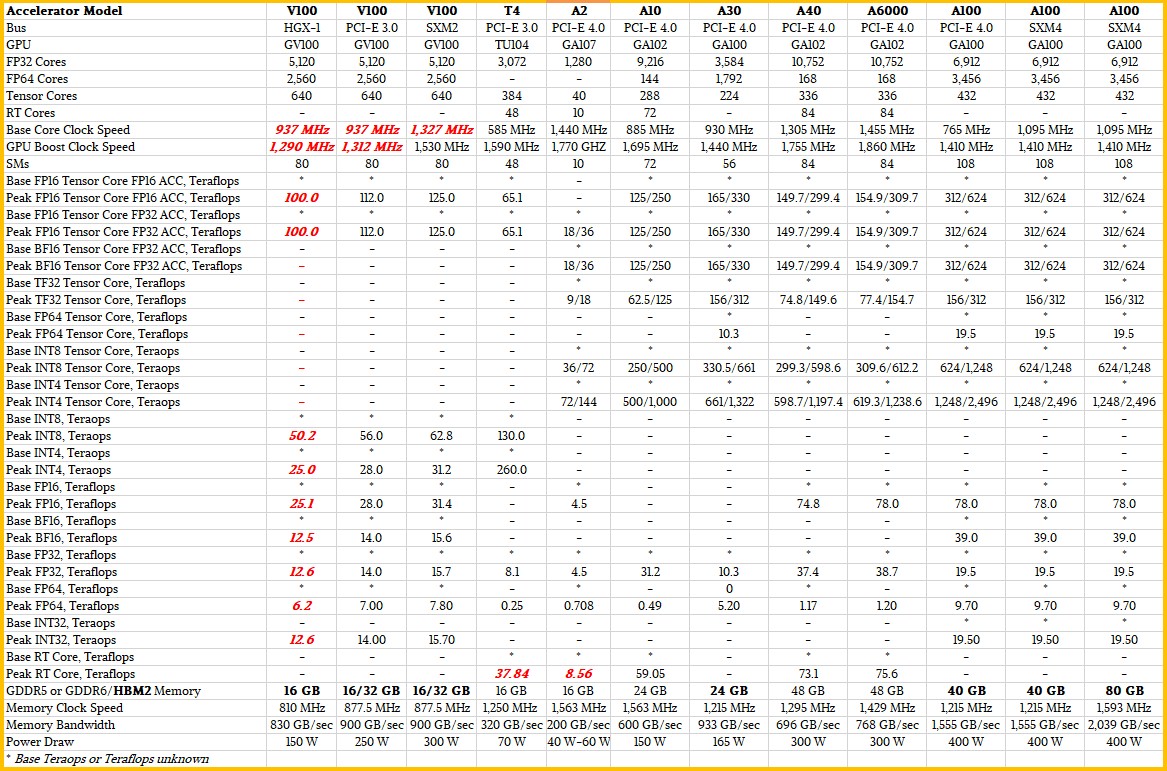
If you click on the table above, you will be able to read it.
Here is a companion table that adds street pricing, as much as we can ascertain it, and does some price/performance analysis:
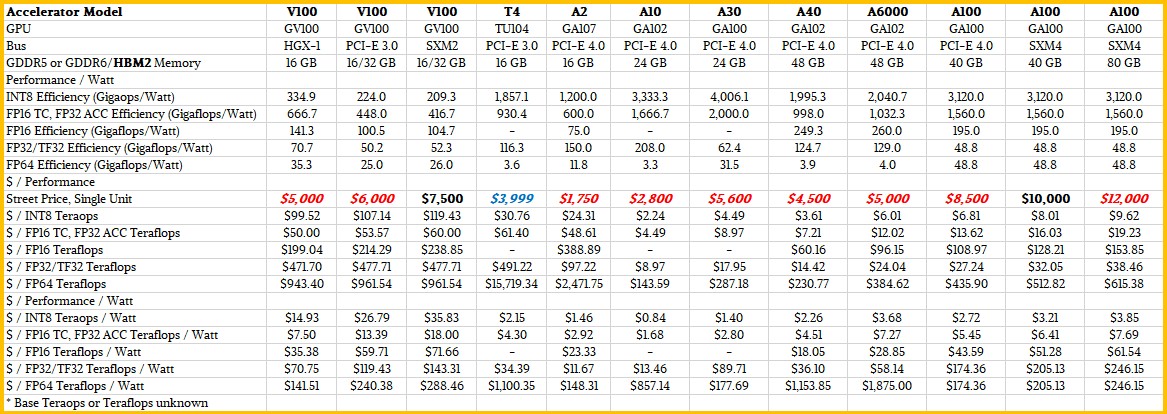
As you can see, the A2 is not a speed demon, but it does have a relatively low price and a very low wattage and even a small form factor size of a half height, half length card that has a PCI-Express x8 slot, and thus even at peak watts and peak performance, it is compact and fairly cheap. And considering that Nvidia has to do something with the dud GA107 CPUs, turning them into A2 inference cards is a perfect kind of recycling. The important thing is that it adds better bang for the buck then the Turing TU104-based T4 accelerator, considerably lower wattage, and we think a much lower price point as well as a small form factor, which the GA100-based accelerators do not offer.
By the way, pricing for Nvidia GPUs is all over the map these days thanks to product supply shortages, which we think are caused by manufacturing and shipping issues thanks to the coronavirus pandemic.
While the A2 will in many cases replace the T4, the real competition is doing inference on CPUs. And here is how Nvidia is stacking up the A2 accelerator on inference work against the A2:
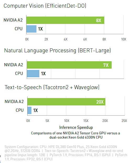
The benchmarks above were run on a two-socket Hewlett Packard Enterprise DL380 Gen10 Plus server with a pair of 28-core Intel “Ice Lake” Xeon SP-6330N Gold processors, which cost $2,029 a pop at list price and which burn 165 watts. The A2 GPU accelerator, we estimate, will cost about $1,750 on the street, considerably lower than the $3,999 we saw for the T4 when we did a price/performance analysis in April of this year and, interestingly, about the same as the pair of Xeon SP 6330N processors used in the Nvidia test. On the EfficientDet-DO computer vision benchmark, a single A2 was able to outperform the pair of Ice Lake processors by a factor of 8X, and bested the CPUs by 7X on the BERT-Large natural language processing test. On the Tacotron2 and Waveglow speed-to-text benchmark test, the A2 speedup over the pair of CPUs was a factor of 20X.
On intelligent video analytics (IVA) workloads, Nvidia adds in its datasheet that the A2 offers 20 percent more performance than the T4 using the ShuffleNet v2 stack and 30 percent better performance than the T4 on the MobileNet v2 stack.
The lesson here is, bang for the buck comparisons between CPUs and GPUs, and across GPU generations and GPU SKUs within a generation, are complex. But that doesn’t mean that system architects don’t have to do the math. Now, there is one more Nvidia GPU accelerator to consider for certain workloads.
The simple math is like this: Throw out one of the CPUs in a server and add A2 accelerators to lower the cost of the node a little and increase the compute density of an inference node. Or, keep the Ice Lake server as it is and pump it full of four or eight A2 accelerators. For latency and security reasons, Intel, IBM, and anyone adding mixed precision vector and matrix math units to their CPUs will argue it makes sense to do this on the CPUs and not offload at all. Those who like the Nvidia software stack for AI training will strongly consider the Nvidia software stack for AI inference, and therefore will take a hard look at the A2 accelerators.

Be the first to comment