

The European Processor Initiative (EPI) has pinned its hopes on RISC-V as the path to European semiconductor independence. The program, which began in 2015 with the goal of building a native exascale supercomputer by 2023, took longer than expected to work out the architectural plan for its RISC-V designs but today did announce progress.
EPI has announced receipt of 143 test chips from GlobalFoundries. The EPAC 1.0 samples have been tested and work, which leads to the question of what lies ahead for Europe and the native HPC system plans it so carefully laid — especially in light of last week’s announcement by Ursula von der Leyen, European Commission President, that Europe should strengthen its role in design and manufacturing of semiconductors by way of a new Chips Act.
This effort will include semiconductor research, production via “megafabs” and a framework for public-private cooperation. Assuming the EPAC 1.0 designs prove robust and viable, one might expect a higher payoff than expected for EPI’s RISC-V efforts, especially for vendor partners SiPearl, Menta, Kalray, STMicroelectronics, and E4 Computer Engineering, among others. These RISC-V designs go beyond datacenter-class processors for the long-heralded native exascale system and are expected to extend to telco, IoT, automotive and other less-powerful devices via a common versus global architecture platform focus.
EPI said that with the successful test of EPAC its next steps will be to “develop, optimize, and validate different IP blocks and demonstrate features and performance of those, thus creating an EU HPC IP ecosystem and make it available to the processor and accelerator industry and academia to create globally competitive production-class building blocks for next generation HPC systems.”
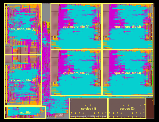
The devices are noteworthy in their heterogeneity and, as one might imagine, pull in IP from various European semiconductor players. As we noted during the FPGA synthesis of the design with the RISC-V ISA at the base, the chips are accelerator driven to meet various application demands. Each had four vector units based on the Avispado RISC-V core as produced by SemiDynamics. The vector units themselves are the result of research at the Barcelona Supercomputing Center.
Each tile also contains a Home Node and L2 cache, designed respectively by Chalmers and FORTH, that provide a coherent view of the memory subsystem. The chip also includes two additional accelerators: the Stencil and Tensor accelerator (STX) designed by Fraunhofer IIS, ITWM and ETH Zürich, and the variable precision processor (VRP) by CEA LIST. All accelerators on the chip are connected with a very high-speed network on chip and SERDES technology from EXTOLL.
The sample run was fabbed on GF’s 22FDX platform and according to EPI, the area is 26.97mm2 with 14 million placeable instances (93M Gate Equivalent) including 991 memory instances, are packaged in FCBGA with 22×22 balls and have a target frequency of 1GHz.
EPI also says the next generation of the EPAC accelerators and interfaces will be improved and refined for even higher performance and lower power levels in 12nm technologies and below, and by adding a chiplet approach.

European Processor Initiative Readies Prototype
Europe is trailing the other major HPC powers in its quest to field exascale supercomputers. The first such European Union machines aren’t scheduled to come online until 2023, at which point the United States, China, and maybe even Japan are likely to have their initial systems up and running. But …
The First RISC-V Shot Across The Datacenter Bow
When it comes to operating systems and now CPU instruction sets, there is proprietary, there is licensable and modifiable with a standard base of functionality with room for some originality, and there is true open source. Which one do you think wins out in the longest of runs? For a …

Ruminations About Europe’s “Alice Recoque” Exascale Supercomputer
Designing chips and shepherding them through the foundry and package and assembly is a complex and difficult process, and not having these skills at a national level has profound implications for the competitiveness of those nations. In many ways, Europe behaves more like a nation than not, and this is …
Be the first to comment