
When it comes to operating systems and now CPU instruction sets, there is proprietary, there is licensable and modifiable with a standard base of functionality with room for some originality, and there is true open source. Which one do you think wins out in the longest of runs?
For a lot of applications in the datacenter over the decades, operating systems have followed this path from proprietary to open systems to open source, moving from stalwart platforms like MVS on mainframes and VMS, OS/400, and MPE on minicomputers that grew into mainframe-class servers, to Solaris, HP-UX, AIX, and dozens of Unix variants that eventually adhered to a common 1,170 APIs to provide a modicum of application portability, and finally to the open source Linux, which started out as a basic Unix-alike kernel and which has grown into a true platform.
Proprietary platforms, most notably Microsoft’s Windows Server but also IBM i and z/OS from Big Blue, still persist and proliferate in the datacenter, and arguably IBM’s AIX, the last standing commercial Unix distribution that is, for all intents and purposes a proprietary platform with the death of Solaris and HP-UX
History doesn’t demand repeating, but it sure looks like it compels it if there are good reasons. It is hard to argue with the philosophy and community of open source, and that is why many of us (including we here at The Next Platform) think there is a kind of inevitability to open source chippery. And hence we are keeping a sharp eye on the RISC-V effort to create an open source chip architecture that spans from the tiniest embedded devices up to massive systems and supercomputers.
But it is important to not get too excited. Architectures and their operating systems persist because it takes trillions of lines of code and tens of millions of programmers to run the world, and you can’t change everything at once. In fact, you can’t change everything over decades. Legacy applications and their platforms persist for good economic reasons, and amortization of investment is just a part of it. Change for the sake of change is not something businesses can afford, and they only change when they really have to.
And so Windows Server is the X86 of operating systems or X86 is the Windows Server of chips, depending on how you look at it, and both will hold some ground against Linux and Arm because no one is going to rewrite a Windows productivity tool set or all those bazillion of lines of code of Visual Basic and C# in the enterprise. Just like some mainframe applications persisted despite the massive pressure of Unix systems, which were arguably better and cheaper platforms on a lot of measures. While RISC had many benefits, enterprises are nonetheless risk averse. Lower the risk, as has happened with Arm server CPUs in recent years with the rise of Amazon’s Graviton, Alibaba’s Yitian, and Ampere Computing’s Altra.
You will, however, always pay a premium for living in the past. And we are seeing this play out on AWS right now as Graviton2 instances offer a 10 percent to 40 percent price/performance improvement over X86 instances for the same amount of work.
In the three and a half decades that we have been watching the datacenter, we developed a rule of thumb that has held pretty true as Moore’s Law and other competitive pressures affected systems. For database processing systems at least, mainframes were roughly twice as expensive as Unix systems per unit of work, and Unix systems were roughly twice as expensive as Windows Server or Linux systems per unit of work. Smaller proprietary systems were initially a tad bid more expensive than Unix, but the few that were left all normalized due to competitive pressures in the late 1990s and early 2000s. Arm platforms could end up offering another 2X step function in price/performance.
The Road From X86 Through Sparc Back To X86 To Arm To RISC-V
If AWS is giving away 40 percent with Graviton compared to X86, you can bet its Graviton platforms are even cheaper than the list price and the company is getting some margin here, too. Or if not, AWS is playing a long game to increase margins even higher later when it controls its own platform.
It is with all of this in mind that we consider Ventana Micro Systems, which dropped out of stealth mode in September 2021 and which has been working diligently on a server CPU design based on the RISC-V instruction set. We caught up with co-founders Balaji Baktha, who is chief executive officer, and Greg Favor, who is chief architect, to get an update on what is now called the Veyron line of RISC-V CPUs that are under development at Ventana.
It is not clear why Ventana has “Micro” in its name – Force of habit? An homage to Sun Microsystems and Advanced Micro Devices as well as Applied Micro Circuits? – because there is nothing at all micro about its aspirations.
Both Baktha and Favor have been down these roads before, trying to push a new ISA into the datacenter. And so they know what to do, and equally importantly, what not to do.
Baktha has along career in the semiconductor industry, and during the Dot-Com boom was one of the co-founders of an iSCSI chip startup that was acquired by Adaptec in 2001, which was eaten by Microsemi. Baktha moved to Marvell in 2002 to run several of its business units for wireless, storage, embedded, and emerging markets, helped run a few companies for a while and then co-founded with Favor a company called Veloce Technologies, started in 2010 and creator of the first 64-bit Arm server and storage chip. Applied Micro bought Veloce in July 2015 and its intellectual property and design team was actually the foundation of the X-Gene product line, which we followed very closely since the founding of The Next Platform over the years. Applied Micro got two generations of X-Gene processors into the field, but did not reach escape velocity and that technology eventually made it through MACOM to be the foundation of Ampere Computing in 2017.
Baktha was a partner at Walden Capital and helped fund startups and was chairman of Apex Semiconductor before co-founding Ventana in July 2018 to do a RISC-V server chip. For the past two years, Baktha has been on the board of directors for RISC-V International, which is roughly analogous a Linux-style community for CPUs.
Greg Favor has crossed paths with Baktha a number of times before, and it is not surprising that they are working together.
Favor started out as a design engineer at Zilog way back in 1983 and then was a senior design engineer at a chip startup called Nexgen Microsystems, which created a series of clone X86 processors during the 586/Pentium generations in the late 1990s that gave Intel some heartburn. After a year at Nexgen, Favor decided to strike out on his own and founded Tera Microsystens in 1989, where he was chief architect of a clone of Sparc workstation processors called microCORE that, interestingly, were fabbed by Hewlett Packard using 1,000 nanometer processes. Favor returned to Nexgen and was there when four years later AMD’s own K5 chip to compete against the Pentium had some issues and the Nexgen RISC-underneath-CISC core approach was brought in. Favor was a Senior Fellow at AMD and drove the K6 design that put AMD on the map as a CPU alternative to Intel.
Like many chip designers, Favor moves around a bit to always have interesting work. He was a processor designer at broadband network chip appliance maker Redback Networks in the wake of the Dot-Com boom, and in 2005, did three years at stealthy CPU maker Montalvo Systems, which Sun Microsystems acquired in 2008 as it was in its death throes looking for a way to save itself. In 2009 as Sun was being eaten by Oracle, Favor moved over to be vice president of processor engineering at – you guessed it – Applied Micro. So in a sense, Favor worked on Arm server stuff that Baktha started many years earlier.
Applied Micro was sold off to MACOM in 2017, but MACOM didn’t really want the X-Gene Arm server chip but its expertise in communication circuits. That is why the X-Gene designs and a lot of the team that created it ended up in the hands of The Carlyle Group to become the foundation of Ampere Computing. Favor stuck around Ampere Computing for a year, took a year off to work on some stealthy stuff, and then in 2019 was a co-founder with Baktha of Ventana.
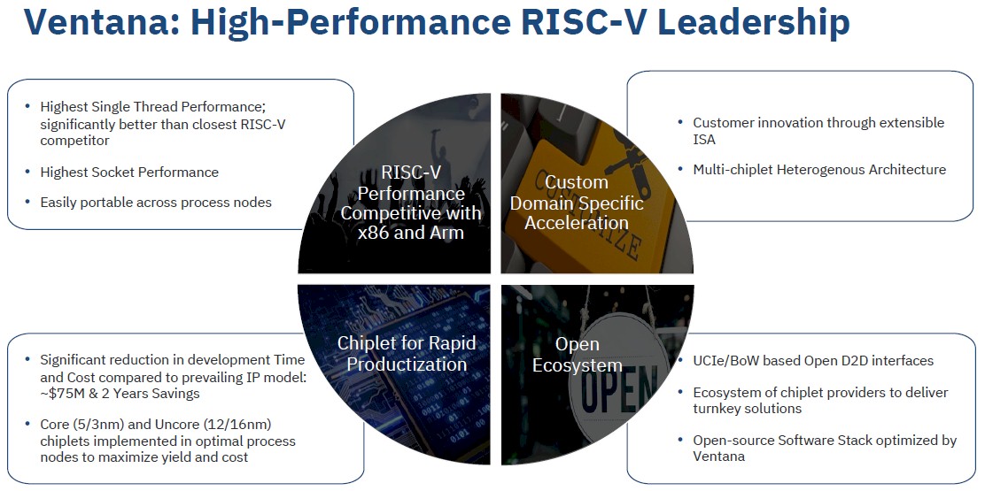
And that brings Baktha and Favor to RISC-V, which many call the fifth generation of the MIPS architecture, and the benefits of a truly open architecture and to escape the tyranny of having someone else completely control what can – and what cannot – be added to an architecture.
With Arm, Baktha says that chip designers like Veloce and AppliedMicro would figure out what the hyperscalers and cloud builders needed, figure out how to implement it, show Arm Holdings how to do it, and then be charged an architecture license fee to access features they helped define and build.
“After spending $100 million on Arm,” Baktha tells The Next Platform, “we realized this is a closed ecosystem, this is not open, and we just went from a monopoly to a duopoly and we realized, okay, enough.”
And so Baktha and Favor grabbed the RISC-V architecture and a bunch of architects and modeled how it might be extended to support various kinds of acceleration above and beyond the CPU core for specific datacenter workloads, and even back in 2018, it could expected anywhere from a 30 percent to 70 percent uplift over the base RISC-V designs.
“As you well know, if you look at the raw performance that you get in a CPU by moving from 16 nanometers to 10 nanometers to 7 nanometers, it was already diminishing,” says Baktha, adding that it is a story that we all know all to well. “You are spending billions of dollars to get an 7 percent or 8 percent performance increase. But by introducing two things – domain specific acceleration and composability – we are able to achieve 30 percent to 70 percent on top of the transistor benefits. But fundamentally, to get there, the table stakes are to come up with a single socket performance number that is on par or better than what X86 and Arm providers can offer in 250 to 300 watts. If you can’t do that, and keep marching ahead, don’t even bother. You also need workload acceleration with a cache coherent architecture. If you don’t do cache coherent architecture, if you are doing two-stage compute – CPU and GPU, CPU to whatever accelerator – that is a loser’s game. So if you can bring in these two things together, you have a winning formula. That’s the founding premise for Ventana to build world-class processor. We set out to do this using 5 nanometer TSMC as our starting point, and we have been able to achieve 3.6 GHz and the power of our core is second to none.”
By starting with RISC-V, Ventana has a clean slate and a highly streamlined instruction set and the Veyron V1processor cores have what Baktha calls “beefy” private L1 and L2 caches for each core. These cores are interlinked with a high performance (and proprietary) interconnect, There is a hierarchy of interconnects, in fact, that allows for 16-core chiplets to be glued together into larger processor complexes, but instead of having one big fabric, which becomes a bottleneck on a lot of architectures, the Veyron interconnect can scale memory, I/O, and chip interconnects such that the cores can be kept fed. The Veyron processors have all of the standard virtualization hooks and memory and I/O interrupts that are expected in a server-class chip.
At the moment with the Veyron V1, Ventana is showing off the design of its 16-core chiplet and is working with an unnamed partner on an I/O die. (Alphawave Semi? Marvell? We are guessing Marvell based on some information you will see in a second ) That would seem to imply that Ventana will be using a NUMA-like approach to building a socket, much like AMD is doing with its Epyc processors, with an I/O and memory die in the center and chiplets of cores hanging off that. But this one has some interesting twists, it looks like.
The Veyron interconnect is a “high performance parallel D2D interconnect” that has the “lowest latency and power” and is “highly scalable,” according to the presentation we were given. And slide this adds some insight:
If you look on the lower right pie slice, you see the bullet that says Veyron will use “UCIe/BoW based open D2D interfaces.” That is very interesting indeed.
You will also see on the right the mix of chiplets used with the Veyron V1 and V2 processors. With the Veyron V1, the core chiplets are implemented in 5 nanometer processes from Taiwan Semiconductor Manufacturing Co with the uncore (meaning that I/O and memory die, as it turns out) being etched in a 16 nanometer process. With the Veyron V2, it looks like the cores with shrink to 3 nanometer processes and the I/O and memory die will shrink to 12 nanometers. We presume that TSMC is the foundry for those I/O dies, considering that GlobalFoundries does not have a 16 nanometer process. (It does have 14 nanometer and 12 nanometer, however.) That mix of nodes aims to maximize the chip yields and also to lower the cost of putting together a compute complex.
Take a look at the Veyron V1 core:
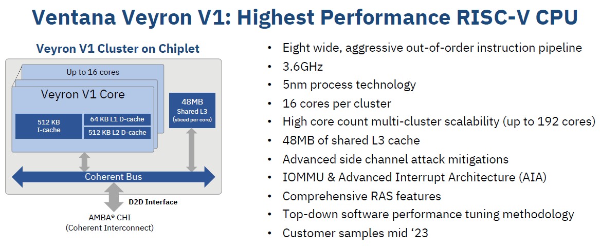
The V1 core sure looks like a modern RISC processor, with an eight-wide instruction pipeline. In 5 nanometers, it can push the clock speed up to 3.6 GHz. Don’t get too excited. That is not the base clock speed with all cores across many core complexes all fired up, which is the clock speed that matters most as far as we are concerned.
Favor says that if customers want to push performance across all of the cores, well above 3 GHz, then you will burn around 2 watts per core. If you can drop down to 2.5 GHz, you will be in the range of 1 watt to 1.5 watts per core. And if you want to have all of the cores running full out and yet keep the thermals down, you can drive it at 1.8 GHz to 2 GHz and still be well under 1 watt per core. Baktha says an X86 core will burn anywhere from 2X to 4X that, given the same performance bands.
“Each core is an aggressive, out of order, high performance, Intel-class performance core,” explains Favor. “When some people say high performance, they don’t really quite mean that. Each core is around two square millimeters, so it is nowhere near as big as an X86 core, and it is single threaded, too, so no hyperthreading. And so every thread is a relatively small but beefy core that is relatively power efficient. And from a cache hierarchy perspective, there’s basically one megabyte of private cash within each core – a half megabyte of L1 instruction cache – and a bunch of patented innovations to enable us to get kind of the benefits of a large first level cache, at the latency of a small cache. And then we have more than a half megabyte of data cache in the hierarchy. Then also a cluster-level shared L3 cache of up to 48 megabytes.”
To be precise, the V1 core has a fat 512 KB L1 instruction cache and a reasonable 64 KB L1 data cache and then another fairly skinny 512 KB L2 data cache. (AMD’s “Genoa” Epyc 9004 and Ampere Computing’s Altra Max have 1 MB of L2 cache per core, and Intel’s “Sapphire Rapids” Xeon SP has 2 MB of L2 cache per core.) But the Veyron V1 has a massive 48 MB of L3 cache per V1 core complex, which is a freaking huge 576 MB L3 cache for twelve clusters of 16 cores and 384 MB for a 8 clusters. Genoa tops out at 384 MB of L3 cache per socket, Sapphire Rapids tops out at 112.5 MB, and Altra Max tops out at a mere 16 MB. If the memory subsystem can keep that cache fed and it is not missing all the time, performance should be a screamer on the Veyron V1. (More on that in a second.)
The neat bit is the coherent bus, and the suggestion that the D2D interface actually implements Arm’s AMBA CHI interconnect interface, and the chart further up suggests that it is running AMBA CHI on a BoW (Bunch of Wires) parallel transport, and specifically the one that the Open Compute Project has been pushing.
“Everything on the core cluster is tied together by a high bandwidth, low latency coherent bus based on an enhanced version of AMBA CHI. But then, the interface from a cluster to the SOC to the rest of the world, if you will, is just standard CHI.
The Veyron interconnect scales up to 12 chiplets in a single socket for 192 cores, but it looks like that full scale will be saved for the Veyron V2. The Veyron V1 that will sample sometime early in the second half of this year will top out at eight 16-core chiplets for a total of 128 cores in a socket. That’s as good as AMD’s “Bergamo” Epyc Zen 4-based X86 server chips coming later this year, as good as what Ampere Computing is doing with its current Altra Max Arm server chips.
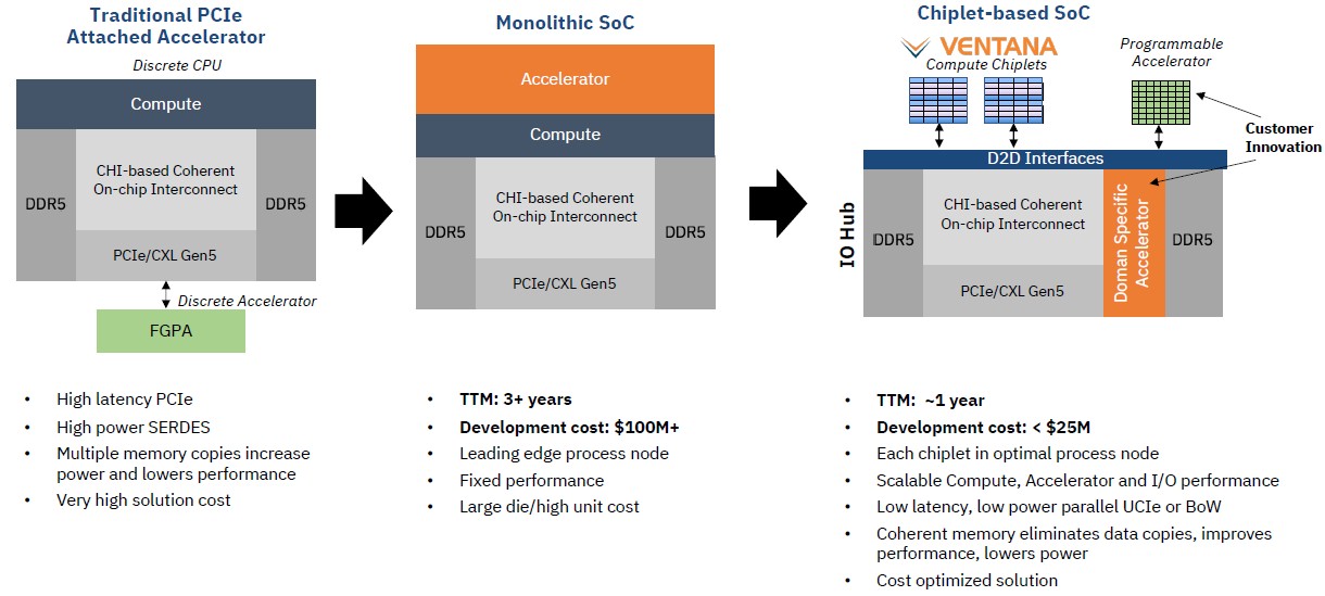
Ventana is not just selling its own full blown server CPU. It has partnered for the I/O and memory die and it has created the V1 cores and it wants to gives customers optional ways to consume it and to save money on bringing a compute complex – and very likely a hybrid one – to market. Customers can license the chip IP, they can buy chiplets and mix it with their own custom I/O and memory hub, (which might have accelerators on it), or they can buy a complex with a specific number of V1 cores wrapped around the I/O and memory hub that Ventana has created with its unnamed partner.
That brings us to performance, and Ventana offers up this chart showing real SPEC integer throughput per socket performance on Intel “Ice Lake” Xeon SPs, AMD Epyc 7763, and AWS Graviton3 processors against the estimated performance of the Veyron V1:
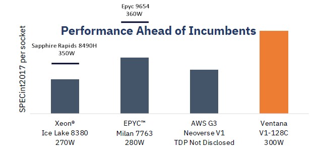
Obviously, we now have newer Intel and AMD chips that will close the performance gap, but clearly, this is pretty damned good for a first pass RISC-V server socket. Just for fun, we estimated where the SPECint2017 performance would be for the new top-bin 60 core Sapphire Rapids Xeon SP-8490H and for the similarly new top bin 96-core Genoa Epyc 9654.
Ventana is shipping development kits for the Veyron V1 based on FPGAs now and will start sample in the third quarter of this year, as early as can be done.
Soon, RISC-V will be off and running in the datacenter. We will be on the lookout to see who is interested, and why.

Talking Datacenter Computing With The CEOs Of AMD And Supermicro
Sponsored Feature: With every server CPU launch, component and system maker Supermicro always wants to be at the front of the line to offer its channel partners and large direct customer base the opportunity to get systems based on the hottest new technologies. And with the 4th generation EPYC processors …
The AI Boom Props Up Datacenter Infrastructure Spending
If there is one thing that is absolutely immune from inflationary curbs and that is, to a certain degree, also contributing to inflationary pressures in the global economy, it is generative AI. In fact, from the limited data we have about server and storage spending in the world right now, …
Intel’s Datacenter Decline Not As Bad As Expected
Incoming chief executive officer and long-time Intel employee Pat Gelsinger is talking the helm of a chip company that has plenty of issues to sort out, but there is some good news as Intel reports its financial results for the fourth quarter of 2020 and Gelsinger gets ready to take …
Nice piece. And I understand that Ventana is already working on a more powerful 2nd generation design, using the RISC-V Vector extension.
MIPS’ RISC-V eVocore P8700 – already available for order – is also worthy of note though:
https://www.design-reuse.com/news/53186/mips-risc-v-ip-core–evocore-p8700-multiprocessor.html
As is Esperanto’s ET-SoC-1, which was being evaluated in the second half of last year, iirc.
I also hear rumours that Alibaba have incorporated T-Head’s chips into their datacentres… but I can’t find proof of that.
I have been wanting to see what Esperanto is up to, and will check out the MIPS P8700. Echoes of HP 9000 in that chip name….
Hi Timothy – great article. Reading through, I found a few typos — I figured I share them with you to edit such a new post:
“Then also a cluster0level shared L3 cache of up to 48 megabytes”
— I think that cluster0level is supposed to be a space.
“To be precise, the V1 core has a fat 512 KB L1 instruction cache and a reasonable 64 KB L1 data cache and then another fairly skinny 512 KB L2 data cache. (AMD’s “Genoa” Epyc 9004 and Ampere Computing’s Altra Max have 1 MB of L2 cache per core, and Intel’s “Sapphire Rapids” Xeon SP has 2 MB of L2 cache per core.) But the Veyron V1 has a massive 48 MB of L3 cache per V1 core complex, which is a freaking huge 576 MB L3 cache for a 12-die complex and a mind numbing 768 MB L3 cache.”
— I don’t understand what you’re saying here … the math adds up in the first part (12 compute die * 48MB L3 / die = 576MB total L3). Where does the mind numbing 768 part come in?
The below thoughts/comments are my own an not a reflection of my company:
Overall – I think it will be exciting for the industry to get its hands on actual devices from these folks and run tests on actual silicon. My guess is there will be some scaling friction in the I/O Die internal fabric going to the 12 compute die shape. Its also curious that there is no provided detail on the memory interface for their IOD partner in the article – did you get that information, or did they not provide? For example… are they targeting DDR5/LPDDR5x/HBM or a mixture? I see a cartoony image that could imply they are targeting DDR5 and PCIe/CXL Gen5, but how many controllers, how many lanes, what’s their SMP strategy (or are they only targeting support for single socket – maybe that’s enough).
Great content – and exciting momentum in the RISC-V space. I think datacenter folks are very risk averse and the uptake will be long and arduous. However, there are many “datacenter adjacent” product markets that could fit this architecture very well (DPU, storage accelerators etc). Thanks for writing the article!
You can always tell when the phone rings in my writing. I am in the middle of something and there are several interruptions and then the error correction doesn’t detect the error. I was thinking about 16 chip clusters and 256 cores and got bollixed up.
If you look carefully at chart three it shows DDR5 memory and PCI-Express 5.0 plus CXL. It is funny to think that this I/O memory hub might be the guts of what might have been ThunderX-4, but with RISC-V cores wrapped around it instead of custom Arm cores.
Thanks – it’s unclear to me if that chart three is an example of what _can_ be done with their compute chiplet, or an actual implementation diagram. I suppose we can wait and see.
Their RISC-V Summit presentation showed their V1 Development platform that includes “128GB single channel DDR5 attached memory using PCIe/CXL Gen5 x16 port” — so I guess that means either they have direct DDR5 controllers in the I/O hub, or are using CXL memory expansion for their memory. I assume the former as they make such effort to claim their BoW D2D has only 7ns of latency (where CXL attached memory would be an order of magnitude or more higher).
I see your points. And agree. It is too early for CXL-only memory ports.
The following excerpt shows, what drives it all:
“Just like some mainframe applications persisted despite the massive pressure of Unix systems, which were arguably better and cheaper platforms on a lot of measures […] You will, however, always pay a premium for living in the past. And we are seeing this play out on AWS right now as Graviton2 instances offer a 10 percent to 40 percent price/performance improvement over X86 instances for the same amount of work. […] For database processing systems at least, mainframes were roughly twice as expensive as Unix systems per unit of work, and Unix systems were roughly twice as expensive as Windows Server or Linux systems per unit of work. Smaller proprietary systems were initially a tad bid more expensive than Unix, but the few that were left all normalized due to competitive pressures in the late 1990s and early 2000s. Arm platforms could end up offering another 2X step function in price/performance.”
…somewhere lost in space, in between of lots of “expensive”, “cheaper”, “price”, “performancce”, there is a
“Advanced side channel attack mitigations”
->It shows the whole problem, the biggest problem. Driven by “more money” and the hybris that we can build our own creation via IT, which then via AI will be our helper and new God in all our problems, we put more and more important parts of life into the IT world and get more and more dependant on it, not seeing that the more we get dependant on something, the more “security” and “safe” should play a role. Theo de Raadt stated correctly, that, with the computing power we have these days (CPU power, SSDs, …) we can easily sacrifice some of this power to enhance security, as security will cost power and performance.
…but perhaps, despite of having lots of “security-detonations” coming nearer and nearer, this re-thinking will happen only, after things crash more heavily than today.
…will we then have enough intelligent people to fix it, or did already everybody rely on ChatGPT or similar, putting the brain on standby, reducing its size, to have more room in the head?
…time will tell…God will show us, that He does not let himself put aside that way…
I think the security angle is interesting. Very interesting. But I also think there was some opportunistic pricing on each legacy platform as the new thing came in, too. Look at the profit margins on mainframes. They could have also cut price and allowed their technology to proliferate and chose not to. For obvious self-interested reasons.
That’s something I forgot to write about in my comment, as there are two sides of each medal: The one, that produces and the one that demands the products.
Yes, you are completely right, they took too much money and misused their position or leadership (“For the love of money is the root of all evil…”). The view from this side I forgot in my comment.
I was also not criticizing you or your article, as you just describe how things are (after having pressed “post comment” I thought “should I have added that it is no criticizing of the author?) and that’s why I read your articles, as one gets deeper information on the technical and business side e.g., where one can draw his own conclusions then about this or that topic (something that get’s sometimes seldom in these days…”everything” is very biased…neutral and purely informal articles are like a breath of fresh air, and your articles are full of, also very interesting background, information).
Didn’t take it as a criticism at all. I just had – not – looked – at – it – that – way, and given that I know about RAS of course that is some of the pricing delta. You and I could chat about what that should be worth as a premium. Not having to change your systems also commands a premium. There is a pain point at which companies will jump. And finally, there is fashion. Sometimes people change things because all of the cool kids are doing it, even if it is disruptive and that disruption eats some of the “cost savings” moving to a new platform.
Appreciate you and your support. Thanks.
Hopefully Ventana’s engineers will borrow ideas from the CHERI research initiative to add more memory safety to C/C++ programs.
What’s the smallest variety of CHERI?
https://msrc-blog.microsoft.com/2022/09/06/whats-the-smallest-variety-of-cheri/