
If the HPC and AI markets need anything right now, it is not more compute but rather more memory capacity at a very high bandwidth. We have plenty of compute in current GPU and FPGA accelerators, but they are memory constrained. Even at the high levels of bandwidth that have come through the use of two and a half generations of 3D-stacked High Bandwidth Memory, or HBM, we can always use more bandwidth and a lot more capacity to keep these massive compute engines fed with data.
There are a couple of ways to deal with the memory bandwidth issue, and memory makers SK Hynix and Samsung Electronics are taking two very different approaches with their future HBM stacked memory. The former is cranking the density and I/O speed up to HBM3. while the latter is going to be embedding processing right inside of an HBM2E memory stack so data does not have to always travel out to a CPU or an accelerator attached to a CPU to be processed and re-stored. In a sense, both are reducing the latency between wanting data for processing and getting it for processing, and it will be interesting to see how this plays out in the market. One approach is more general purpose while the other is going to be application specific, and we always like the more general approach if we can have it and accept the specific approach when no alternative appears to drive price/performance.
Very little has been said about the future HBM3 standard, and that stands to reason with only three suppliers of HBM memory: Micron Technology, Samsung, and SK Hynix. They all want to keep their secrets under wraps for as long as possible while at the same time driving the JEDEC memory standards that govern HBM.
In general, HBM memory allows for four, eight, or twelve DRAMs to be stacked atop each other and linked to each other with through-silicon vias, or TSVs, which is a finny way of saying wires that are built up in the DRAM memory dies themselves and linked to each other in the stack through the same kind of microbump connections that are used to link chips to each other and to motherboards. With HBM, an interposer is used to link the compute elements to the memory.
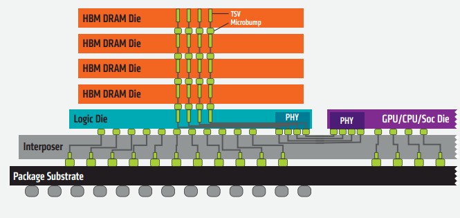
While HBM1 (no one calls it that, but we are going to) had AMD and then Nvidia as users for their GPU cards, it wasn’t until HBM2 came along that the cost came down and the technology matured enough for even CPU makers to consider using it. With HBM2E, the latest greatest variant of HBM, the bandwidth and the capacity have both gone up a little, and the HBM stacks are getting taller, too.
HBM1 had a 1,024-bit bus width, and a four die stack running at 500 MHz could deliver more than 100 GB/sec of bandwidth per stack, which was quite a bit more than the 32-bit GDDR5 memory, which was a lot less wide but which ran at 1.75 GHz and delivered 28 GB/sec per chip. The GDDR5 memory of equal capacity took up 19.2X more space (on a 1GB chunk) and burned more than three times as much electricity, too. HBM1 was expensive, and tough to manufacture, and that is why we did not see it on every device that could have used it. The HBM1 stack had four dies and two 128-bit channels per die or 1,024 bits, and putting four stacks on a device yielded 16 GB of total memory and 4,096 bits of memory width, which is eight times that of a 512-bit wide memory interface for GDDR5. HBM1 supported 1 Gb/sec signaling rates on each pin, which yielded 128 GB/sec on a 4 GB memory stack.
With HBM2, the signaling rate was boosted to 2 Gb/sec and with the same 1,024 bit width on a stack that meant a package could drive 256 GB/sec per stack. So four stacks gets you to that magical 1 TB/sec of aggregate memory bandwidth, and at 8 GB per stack (with right high stacks) that gives a 64 GB potential maximum capacity as well. No one, to our knowledge, put HBM2 into production with all eight stacks.
That is not the case with HBM2E, the extended version of HBM2, the signaling rate was boosted to 2.5 Gb/sec per pin and up to 307 GB/sec of bandwidth per stack. In theory, the stacks with HBM2E can be twelve dies high, boosting capacity to 24 GB using 2 GB HBM memory DRAMs. Both SK Hynix and Samsung have surpassed these levels. Samsung’s HBM2E stayed with eight dies per stack and a 3.2 Gb/sec signaling rate, which works out to 16 GB per stack and 410 GB/sec per stack, while SK Hynix cranked the signaling rate up to 3.6 Gb/sec and kept the same 16 GB per an eight stack and a bandwidth of 460 Gb/sec per stack.
HBM3 is a bit of a mystery still, but SK Hynix gave some hints recently in this post about what it was doing for the HBM3 generation.
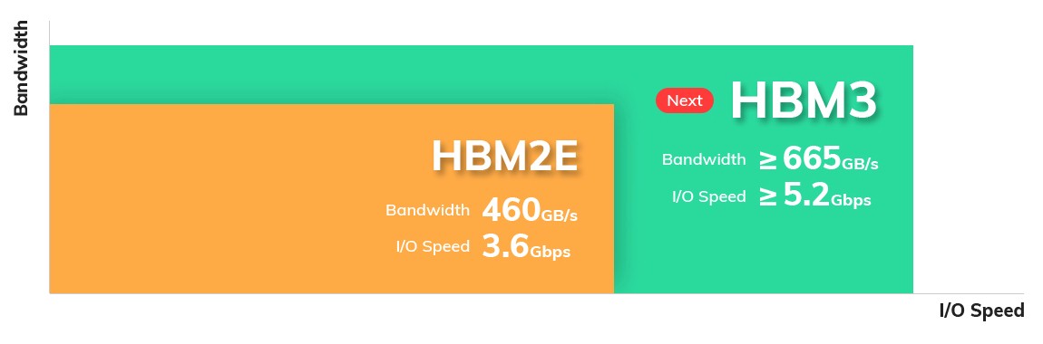
What the company promises is that its implementation of HBM3, which is expected in systems in 2022, will have a signaling rate in excess of 5.2 Gb/sec and will deliver more than 665 GB/sec per stack. To drive capacity, SK Hynix says it can stack the DRAM chips up to 16 dies high, and if the memory capacity can double again to 4 GB per chip, that will be 64 GB per stack and across four stacks that will be 256 GB of capacity and a total of at least 2.66 TB/sec of aggregate bandwidth.
That is going to be amazing, and even at half the capacity and most of the bandwidth, this will be transformative for HPC and AI computing. We are just getting a taste of this with the Nvidia and AMD GPUs, the NEC Aurora vector engines, the Fujitsu Sparc64-IXfx and A64FX processors, and the future Intel “Sapphire Rapids” Xeon SP processors that all have HBM2 or HBM2E memory on them. We will all want laptops with 8 GB of HBM3 memory, and I would gladly pay the premium – especially if that same memory can be shared between the CPU and the GPU. We expect that some variants of HBM3 will use a 512-bit bus and not require an interposer, and that others might use an interposer to double up the bandwidth and the capacity. So the laptop with HBM3 is not necessarily crazy. Nor is a regular GPU card if this turns out to be true.
Which brings us to the point we are trying to get to. Imagine if any solver and any reasonable chunk of data to be processed against it in the HPC or AI application ecosystem can easily fit inside of HBM3 memory and does not really need standard DRAM memory on the CPU any longer? Maybe standard DRAM is the new flash, and especially something like 3D XPoint memory, if it survives, will be the only “DRAM” that a system will need. It is something worth thinking about, if the price/performance curves come down as we expect they will. Standard DRAM will always be cheaper, but so is tape compared to disk and disk compared to flash and flash compared to DRAM or 3D XPoint. While plenty of systems will get by with plain vanilla DRAM, maybe all future HPC and AI systems will have HBM on their CPU, GPU, and FPGA components, and we will be talking about how to make coherent links across those HBM3 banks.
Maybe Samsung has a point, too, by moving processing inside of the memory, which we have written about a bunch of times here. AMD was working on processing in memory, or PIM, techniques for its Fast Forward and Fast Forward 2 research projects for the US Department of Energy, and more recently Upmem, a French memory maker, has done its own twist on the idea. A few years back we covered some survey research done at the University of Wisconsin that examined a lot of the PIM projects, if you need a refresher.
The Samsung HBM-PIM device will add 1.2 teraflops programmable computing units between the memory banks and the TSVs. This shows what looks like two banks of compute and eight banks of memory in a stack:
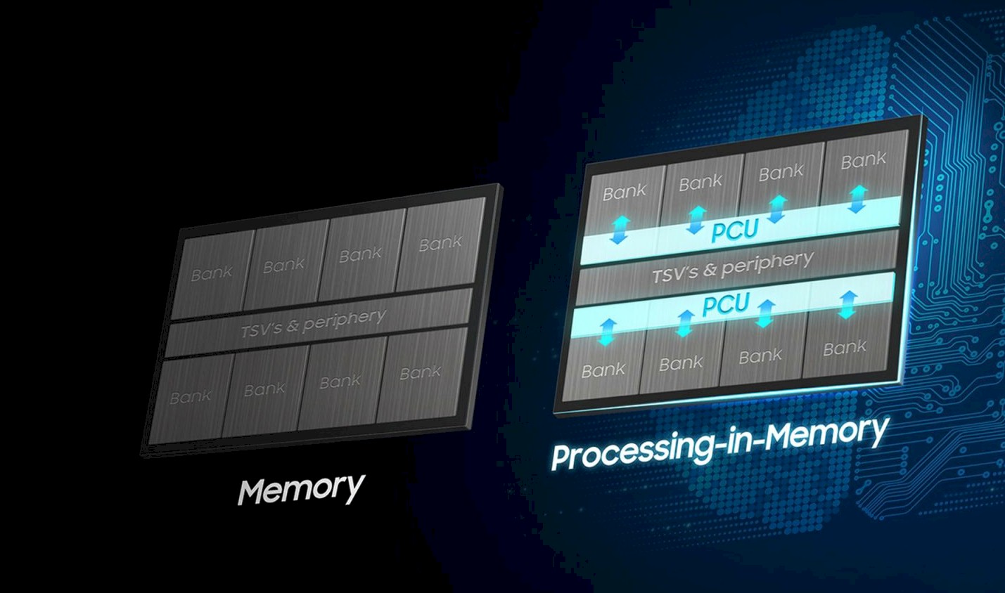
Samsung is saying that the HBM-PIM memory will boost overall system performance on AI workloads by 2X and cut power consumption by 70 percent versus systems that use HBM memory on their accelerators.
Hopefully, both companies will be saying more soon about their HBM3 and HBM-PIM plans. You have our attention, even if we are skeptical of the broad applicability of a universal matrix math engine that is embedded in memory. We would love to be proven wrong here, and see the birth of a new kind of distributed, hybrid computing.

AMD Makes A Big DPU Move With $1.9 Billion Bid For Pensando
Lisa Su has had the datacenter in her sights since taking over as president and chief executive officer of AMD in 2014, charting a course that would allow the processor maker to once again become a factor in the global server market after a decade or so in the wilderness …
Now Comes The Hard Part, AMD: Software
From the moment the first rumors surfaced that AMD was thinking about acquiring FPGA maker Xilinx, we thought this deal was as much about software as it was about hardware. We like that strange quantum state between hardware and software where the programmable gates in FPGAs, but that was not …
Picking Apart AMD’s AI Accelerator Forecasts For Fun And Budgets
Given two endpoints and a compound annual growth rate between those two points over a specific amount of time is not as useful as it seems. Not when you are trying to figure out what is happening at all of the points in between. And that is necessarily so because …
“We will all want laptops with 8 GB of HBM3 memory, and I would gladly pay the premium – especially if that same memory can be shared between the CPU and the GPU.”
HBM Memory like GDDR graphics memory appears to be optimized for bandwidth at the cost of Random R/W access latency so maybe that’s not the best for Consumer Laptop SKUs that need the better Random R/W latency that the nominal CPU memory provides. Now for APUs/SOCs with Integrated Graphics HBM2 would be a game changer there and if the CPU can be given sufficient L3 cache to effectively hide any of the HBM memory’s inherent random R/W latency disadvantages to the CPU’s cores that need that then fine there for the CPU/GPU sharing of HBM access.
More L3 can really help the for Latency and even Bandwidth advantages compared to any off die memory so AMD’s V-Cache there for APUs and the CPU cores working from L3 and not any off Die Memory as much as possible is best. So for Laprops a single stack of HBM2/3 and even at 4GB that’s sufficient for the needs of any Integrated Graphics while the CPU can get more L3 there but will still need access to some expandable/replaceable LPDDR5 memory.
HBM doesn’t have a RW latency penalty compared to DDR – it’s descended from DDR4LP if I remember right.
The main issues with HBM are
(a) density
(b) parallel organization – 8 independent channels (optimal configuration is to treat each channel as a pair of pseudo-channels).
The parallel organization makes sense when there is a parallel (and memory-bound) workload. GPUs yes, laptop CPUs no. HPC multicores yes (some Xeon Phis had it, I think). FPGAs – of course.
Workloads that can’t make concurrent use of the HBM channels will get equivalent benefit from using 32 bit wide DDR5.
PIM has been the future of HPC since the ’90s. All sorts of DOE/Nasa/DOD studies saying the only way to get to petaflops was with PIM. Except no one could figure out how to effectively program them. Maybe someone will figure it out someday. Given the number of HPC systems that still don’t use GPUs because they’re too hard to program, it might be a while.
I believe NVIDIA never used the original HBM. NVIDIA’s first use of HBM was the P100 which uses HBM 2. I think HBM was limited to 4 GB of capacity.
Nvidia only ever had working protypes of P100 with HBM1. I can’t find any evidence of it going inot large volume production cards. Re:
https://videocardz.com/58743/nvidia-pascal-prototype-gpus-analysis
I believe AMD got 8 Hi-Stacks of HBM2 into production with their Vega Frontier and MI25 cards. They had two stacks totalling 16GB. Also, They had 32GB on four stacks with the MI50, so I guess that counts as well.
Dick Sites, DEC, 1996, “It’s the bandwidth, stupid!”