
From a conceptual standpoint, the idea of embedding processing within main memory makes logical sense since it would eliminate many layers of latency between compute and memory in modern systems and make the parallel processing inherent in many workloads overlay elegantly onto the distributed compute and storage components to speed up processing.
This is the founding principle of a French startup called Upmem, which uncloaked its processing in memory, or PIM, modules last year at the Hot Chips 31 conference last summer at Stanford University. Last summer, Upmem had created some PIMs and was giving them out to early adopters to play around with, and now the company has put together some early benchmarks that show off the benefits of the processing-in-memory approach.
There are all kinds of data processing systems that move the compute closer to the data – databases have been doing all kinds of tricks to move data closer to compute for decades within a single system through various kinds of caching, sharding, and indexing, and the Hadoop analytics framework literally dispatched compute tasks on chunks of data to the servers that had the disk drives that had that data. In these and others cases, the idea is that you move the compute to the data, not the data to the compute as is typically done in a standard server and its software stack.
But with the PIM architecture that Upmem has created, data processing units, or DPUs, are not on the system bus or even the other side of the memory bus, but are etched into the memory chips themselves, which are then soldered onto the DIMMs just like any other memory. The distances between the DPUs and the memory cells in the DRAM chips are short, and so the energy to move that data back and forth between the PIM compute circuits and the memory cells is very small. That means it does not take huge amounts of energy and that the latencies, at least on the PIM itself, are very small. The PIM memory remains just as far away from the CPU hosts and their various levels of cache, and storage outside of the cache and main memory remains just as far away on the PCI-Express bus.
Upmem started sampling its 8 GB PIM modules last fall, which have eight DDR4 memory chips with a total of 64 DPUs on each side of the module, for a total of 16 chips and 128 baby compute elements on a two-sided module that delivers 8 GB of capacity at a cost of around 10X of regular 8 GB DDR4 DIMMs. The memory runs at 2.4 GHz and the DPUs run at 500 MHz. We went into the architectural details last summer and we are not going to get into all of these again right here. But two points bear emphasizing again. The first is the architecture of the in-memory compute and the other is the expected incremental cost of that compute.
The DPUs in the PIM use the asynchronous interfaces that memory chips use to talk to each other, and this increased the complexity of the compute logic design. But by sticking with the DRAM interfaces, the DRAM part of the chip can essentially be left alone, and this is valuable. The DPU has a 14-stage pipeline, which has to be deep because the clock speed is, at 500 MHz, pretty low. The DPU has 24 hardware threads in it, which is a big number by CPU standard, and it can hit peak processing performance with 11 or more of those threads are humming. The DPU can do one instruction per cycle on multithreaded code, and the bandwidth between the DRAM cells and the DPUs on each Upmem chip is 1 GB/sec; data can be transferred in anything from 8 B to 2 KB chunks. The DPU does not have data or instruction caches akin to those in a CPU, but has an explicit memory hierarchy that can use DMA operations to move data between DRAM and a 64 KB write memory (SRAM) and a 24 KB instruction memory (also SRAM). There are too many threads in the DPUs to have a complex cache hierarchy like CPUs do.
Now, for cost. PIM memory is pretty pricey now, but it will come down over time if the idea takes off. Gilles Hamou, co-founder and chief executive officer at Upmem, told The Next Platform last summer that with volume production, Upmem thought it could drive the PIM price premium over standard DRAM down to about 50 percent, which is very reasonable considering that fat memory sticks at 64 GB would have eight times as much capacity and hence would have a fairly large distributed compute capacity embedded within it. More importantly, with higher capacity and more compute, parallel workloads running on a dataset of a given size should finish more quickly as the PIM density – and therefore its compute capacity – ramps. This is provided that Upmem keeps the ratio of compute to capacity the same rather than holding the compute steady and increasing the density of the memory cells only.
Upmem had made some estimates of how its memory might accelerate performance for various kinds of workloads, but Hamou reached out to us now that Upmem has some actual benchmarks. Take a look at this chart and we will explain what is going on:
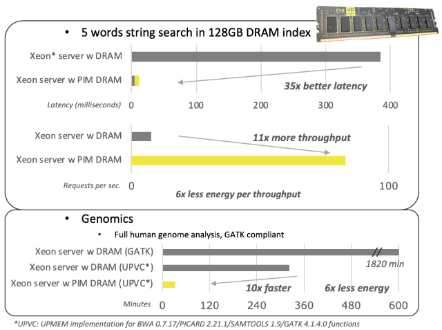
On the first benchmark above, this was actually performed at a real-world customer that runs search engines that Upmem is not allowed to disclose, but conceptually think of this as running Lucene or Elasticsearch. For these search engines, the indexes for the search engines – the result of chewing through raw data on the Internet and creating addresses for all relevant hits on those terms on all of those Web pages that have been indexed – are already running in DRAM to speed up the search.
“With search engines, performance is critical,” Hamou reminded The Next Platform. “Milliseconds are money in this workload, and so you have to look at both latency and throughput of a system running a search engine. So we are not only looking at making applications more productive with higher throughput, we are also looking at making them faster with lower latency.”
With the PIM architecture, there are 64 DPUs per physical memory chip, which works out to 64 MB memory chunks per DPU, and in the search engine case the index is sharded and spread evenly across these chunks for the total capacity of 128 GB in the two-socket Xeon server used in the test (that’s eight memory slots per socket).
“You have to be cognizant of data locality in this splitting of the index,” says Hamou, because you need to get data to a total of 2,048 DPUs within the machine. “We split the database in such a way that statistically, all of the DPUs, within a few percent, will take the same time to go and get back a result. The results come back in about 12 milliseconds instead of 385 milliseconds – a factor of 35X in our test. And the throughput, which again depends on the multithreading and the parallelization, is 11X higher in this first implementation. This latency and throughput are huge advantages for any search engine, and it is acceptable to do this tuning manually for now given these advantages. In the future, we will have embedded memory libraries that will automatically split the search engine indexes within machines and across them.”
Before too long, it might take a lot less computing on the server to get a given search engine throughput and latency using PIMs compared to conventional servers with just DIMMs, although Upmem did not test this idea out or look at the resulting economics. But even if the memory turns out to be 10X as expensive today, if it can do 11X more throughput, it balances out, and if the latency is 35X better, then customers are that much more happy. As the Upmem memory scales up to fatter capacities and more embedded DPUs for compute, it will take fewer and fewer servers for a certain sized search index to fit into, and we suspect also require machines with fewer and few CPU cores. There is possibly a crossover point where the CPU is not really doing all that much, the sharding of the index across the PIMs is automated, and the cost and hassle of running a search engine with its data and its processing largely in memory has the same cost – or less considering the high bin parts Google, Microsoft, and others use for search engines – with a lot more throughput and a lot zippier response time.
In the second part of that performance benchmark chart, Upmem tested a genomics sequencing workload using the Genome Analysis Toolkit (GATK) from the Broad Institute, which is the touchstone for accuracy in genome analysis. And running against GATK, the GATK test took 1,820 minutes to complete on that two-socket Xeon SP server using 128 GB of DRAM. Upmem, with the help of an unspecified customer, tweaked the genomics stack to run considerably faster on this server (at what we presume is a slightly lower accuracy level than the GATK touchstone to speed up the test), and it could finish the job in 320 minutes. Now, adding the PIM memory and offloading the genomic sequencing calculations to the DPUs cut that down to 32 minutes, and the resulting calculation – presumably because the CPUs were mostly idle – consumed one-sixth the energy. (Precisely how this happened was not divulged.)
Hamou says that Upmem is delivering samples to a limited number of customers (including a lot of research labs) as well as partners across the globe, with the heaviest interest coming from the United States and we suspect more than a few hyperscalers and cloud builders, who are always looking for some kind of edge. The first generation of Upmem PIMs will move into mass production in June and July, and from there it will be a matter of ramping up the memory and compute density on successive generations of DIMMs. It would not hurt to get on track for the future DDR5 memory, which is expected to have memory buffers implemented in a non-invasive way to help boost system throughput.
We wonder just how many CPU cores could be replaced by this in-memory compute. You might have a smaller number of overclocked cores running on the CPU and let these other routines run massively parallel in memory. Upmem has said in the past that the Upmem DPU at 32-its has about one-sixth the performance of a 64-bit Xeon SP core, and if you do the math on that, then the computation included in the 128 GB of PIM memory is roughly equivalent to around 340 Xeon SP cores. That’s crazy.

What Faster And Smarter HBM Memory Means For Systems
If the HPC and AI markets need anything right now, it is not more compute but rather more memory capacity at a very high bandwidth. We have plenty of compute in current GPU and FPGA accelerators, but they are memory constrained. Even at the high levels of bandwidth that have …
Data Locality is more about the cost of taking an action. In Hadoop, the cost of moving the code to the server where the volumes of data resided, was cheaper than moving 10’s of GB or more data to where the processor resides.
In 2011-12, Boris Lublinsky and I did some research, which we published on InfoQ where we had an example where the cost of the compute was greater than the cost of transporting the data, so that shipping the data across the network was actually cheaper. This lead us to question the value of data locality.
Networking is also something to consider. Improvements here also called in to question the issue of data locality.
While I find the concept behind these chips interesting, I would have to assume that their viability would be dependent on the use cases…
Interesting none the less…
Is there any concerns on security?
What if intruders managed to launch a task running in the DPUs and steal the data.
What kind of protection do they have?
The concept of PIM has been around since forever. But there are many problems with it that have prevented it from becoming widely used:
1. There are just a few vendors that have high-density DRAM process – Hynix, Samsung, and Micron. Any would-be chip house that wants to do a PIM design would have convince one of these vendors to work with them and offer up a design kit that can target the specific process. Unless these vendors are willing to work with you in a serious way, you’re basically dead.
2. The logic capabilities of a DRAM process are quite limited compared to an ASIC/CPU process. Density is bad. Frequency is slow. Interconnect is limited (due to only 3 levels of metal)
3. Many serious applications requires pulling large amounts of memory from many memory chips into a central location and doing processing of the data. Requiring all processing to be done remotely is a major change in programming paradigm.
4. Unless there is special emphasis placed on inter-chip communication, it is not possible to communicate between PIM chips in such a way as to be able to process many workloads. The PIM chips in this article suffer from this problem – i.e. the DDR4 memory interface is not an effective communication fabric for general purpose inter-chip communication. It’s great for fetching or storing memory chunks from a central master, but not for peer-to-peer communication as is required for most applications
5. The cost of custom memory chips is much higher than regular memory chips and there is no reasonable scenario for it coming down to anything less than 5X. Even HBM is several times the cost (on a per-bit basis) than regular DDR and HBM is still commodity.
Overall, if one is willing to pay additional cost, there is a strong argument that HBM-style multi-chip packages are a better answer than PIM. You get the advantages of ASIC/CPU process for the processing component and the benefits of relatively tight coupling and high bandwidth to the memory banks afforded by the 3D chip stacking and on-package integration of HBM. On top of that, you get at least some cost advantages due to semi-commoditization of HBM versus a custom DDR chip.