
Perhaps the biggest task that processor and system designers have to wrestle with these days is how to keep heavily cored and massively threaded processors fed with data. Modern CPUs have anywhere from 24 to 64 cores, from two to eight threads per core, and run at 2 GHz to 4 GHz, all depending on the architecture. It takes an incredible amount of orchestration – and energy and time – to get data from storage into memory so it can actually be processed.
The logical thing – for certain kinds of algorithms at least – would be to do the processing inside the memory, thus eliminating some of the costly data movement and massively improving the overall efficiency of computations. This approach is called processing in memory, or PIM for short. And a French upstart called Upmem has launched special DDR4 DRAM that has data processing units, or DPUs, etched inside the memory using the same processes that the DRAM transistors are etched in.
Think of Upmem’s implementation of PIM, which was unveiled at the recent Hot Chips conference at Stanford University, as a kind of accelerator that doesn’t hang off the CPU’s host bus, or even the memory bus, which is much faster, but resides right inside the memory itself. The distances between the DPUs and the memory cells in the DRAM are short and the energy to move that data back and forth as it is being calculated upon is small. The latencies are ridiculously small, and that means calculations can finishing quicker and be done in parallel across massive banks of memory, which also frees up the CPU cores to do other kinds of serial and vector work that they are best suited for.
Here is how Fabrice Devaux, co-founder and chief technology officer at Upmem, did the comparisons between PIM processing using the Upmem devices and standard CPUs in servers. The server data is a little bit old, and we think it is being generous to the server processors, memory controllers, and DRAM, which all run a lot hotter here in 2019 than they did using the data gathered by John Shalf of Larence Berkeley National Laboratory back in 2013 about the energy consumed to do work on CPUs. Anyway, here is how PIM stacks up against CPU processing:
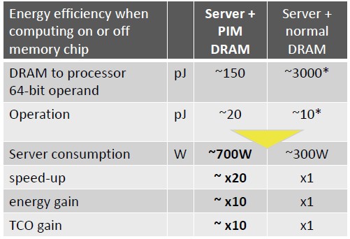
To move data from DRAM memory on the PIM modules to one of the adjacent DPUs on the memory chips takes about 150 picoJoules (pJ) of energy, and this is a factor of 20X lower than what it costs to move data from a DRAM chip on a server into the CPU for processing. It takes on the order of 20 pJ of energy to do an operation on that data in the PIM DPU, which is inexplicably twice as much energy in this table. The server with PIM memory will run at 700 watts because that in-memory processing does not come for free, but we also do not think that a modern server comes in at 300 watts of wall power. With middle bin Xeon SP processors and a fair amount of storage, it is probably closer to 450 watts, and for top bin parts it will easily be 600 watts. Adding PIM memory to such machines would add even more heat, of course. But over time, as PIM memory gets more dense and has more memory and compute on each DIMM, then the TCO gains will be something on the order of 10X.
That is not, by the way, happening today with Upmem’s first PIM modules. Gilles Hamou, co-founder and chief executive officer at Upmem, tells The Next Platform that the initial 8 GB DDR4 memory modules that the company is sampling now with embedded computing on them cost about 10X that of equivalent DRAM memory modules. But, Hamou adds quickly, with volume production and denser memory, that price differential can be brought down to a 50 percent premium, which is tolerable given the massive and embarrassingly parallel computing that will be available inside the memory and accessible through normal C programming.
There are a bunch of things that have to be balanced out to create a PIM module, explains Devaux. But the important thing was to create the PIM using up-to-date, unmodified DRAM process technology, to use mainstream memory interfaces, and to support traditional and popular programming languages used for those creating high performance applications – meaning C or C++.
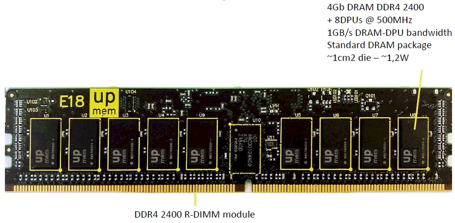
There are some challenges to putting processing right on the DRAM chips. First, on the same process, the transistors used in memory are three times slower than the transistors etched for CPUs, and moreover, the transistor density is about an order of magnitude less than it is on those CPUs. So that is a factor of 15X difference in potential compute throughput. The 4 Gb memory DDR4 chips that Upmem has created run at 2.4 GHz and have eight DPUs running at 500 MHz; it is implemented on a registered DIMM module with nine chips per side (eight for data and one for parity for error correction) to deliver 4 GB per side for a total of 8 GB of capacity. Each Upmem 4 Gb DRAM chip has around 1 centimeter square of area and burns about 1.2 watts. There is a controller chip on each side of the module as well. Like this:
The other big difference is that memory chips don’t have as many metal layers – three versus anywhere from 10 to 17 with modern CPUs – so the routing density between components is also a lot lower. Memory wafers are about half the cost as compute wafers, says Devaux, so that mitigates against some of the throughput differences between in-memory and CPU computing.
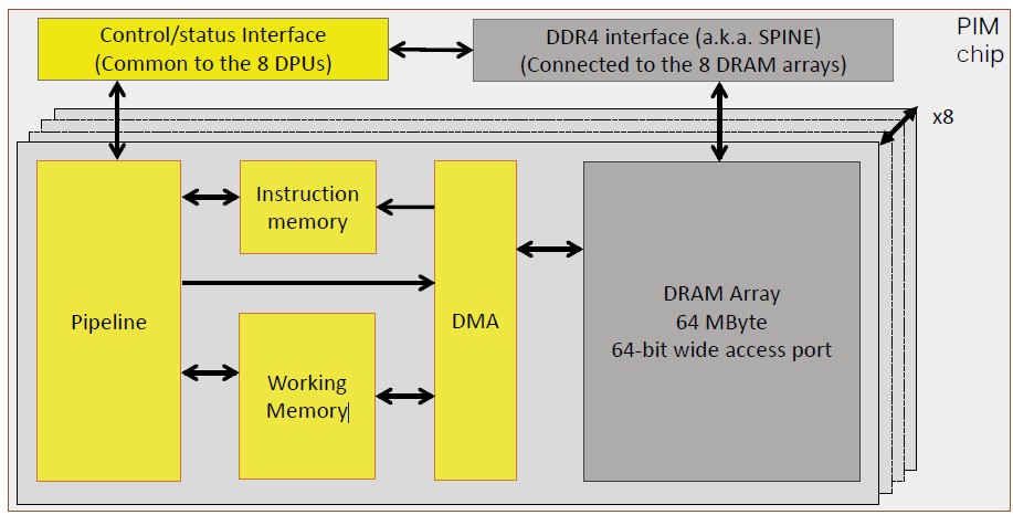
The idea with the DPUs on the Upmem chips was to make use of the asynchronous interfaces that memory chips use, and this increased the complexity of the logic design. But by sticking with the DRAM interfaces, the DRAM part of the chip can essentially be left alone, and this is valuable. The DPU itself has a 14-stage pipeline, which had to be that deep because the clock speed is only 500 MHz. The DPU has 24 hardware threads in it, which is a huge number, and it can hit peak performance with only 11 or more of those threads are humming along. The DPU can do one instruction per cycle on multithreaded code, and the bandwidth between the DRAM cells and the DPUs on each Upmem chip is 1 GB/sec; data can be transferred in anything from 8 B to 2 KB chunks. The DPU does not have data or instruction caches akin to those in a CPU, but has an explicit memory hierarchy that can use DMA operations to move data between DRAM and a 64 KB write memory (SRAM) and a 24 KB instruction memory (also SRAM). Devaux says that there are too many threads in the DPUs to have a complex cache hierarchy like CPUs do.
Here’s the block diagram of the PIM device:
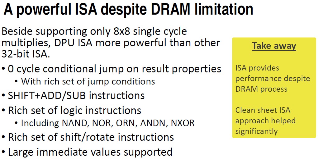
The DPU is not based on the Arm or the RISC-V architecture, but rather on a proprietary 32-bit instruction set that Devaux says “is almost RISC.” This DPU is only good for scalar, in order, and multithreaded code that has good thread context and it is a “clean target” for LLVM/Clang compilers. On the host side, the Upmem SDK can compile 64-bit C code so it can offload calculations to the Upmem DPUs, and Hamou says that programmers have to care about data locality – presumably there is some way to pin the C code to specific memory blocks, just like is done with processors and memory chunks on NUMA servers.
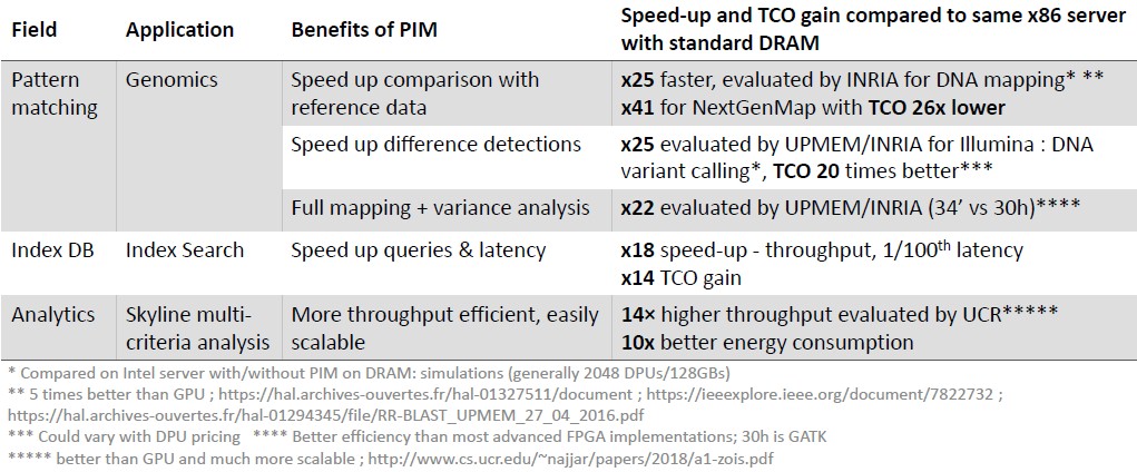
On branchy integer code – the kind that is expected to be used on the PIMs – Devaux says that the DPU on each chip has about 1/6th the performance of a Xeon SP core. Here is a sampling of the speedups that Upmem has seen on various kinds of code, running on a two-socket Xeon server with 128 GB of regular DDR memory versus the same machine running with 128 GB of Upmem PIM memory with 2,048 DPUs acting as compute accelerators:
By the way, the DPUs, by definition, are isolated from each other and do not share data, so there is no chance of the side channel attack as can happen with processors that support speculative execution. (Meaning all of them for the past two decades, pretty much.) The DPUs are linked over the memory bus to the CPUs, which offload chunks of code to them much as CPUs do with GPUs, only in this case there is no copying of data between distinct memories. Everything is already in DRAM or can be pulled into it.
The first generation of Upmem PIMs are etched in a 25 nanometer process; we don’t know who is the foundry is. (Samsung, Micron Technology, or Intel are the obvious possibilities. There is one DPU core for every 64 MB of memory, so memory and compute scale linearly with each other inside the Upmem PIMs and as more PIMs are added to a server, too. There are eight DPUs per 4 Gb DDR4 memory chip, and the R-DIMM has a total of 8 GB of capacity and 128 DPUs with 16 chips back and front. On a server with 16 DDR4 memory slots, that yields 128 GB of capacity and 2,048 DPUs with an aggregate memory bandwidth of 2 TB/sec between the memory chunks and the DPUs. X86, Arm, and Power9 processors are currently tested and supported using the Upmem PIMs.
That is roughly twice as high as you can get with a GPU and its HBM2 memory. You can, of course, add multiple GPU accelerators to a system an interlink them with NVLink if they are from Nvidia or Infinity Fabric if they are from AMD, so with four or eight or sixteen GPUs, the GPUs will win the aggregate memory bandwidth throwdown. But Upmem can start cramming more compute onto its chips and more chips on a DIMM – perhaps by stacking them up as some server memory makers do – and keep pace. We will see what Upmem will do.
The Upmem PIMs are sampling now and there is also an FPGA simulator that can run on a host FPGA card using a Virtex FPGA from Xilinx or on the F1 FPGA instance on the Amazon Web Services cloud. The f1.16x-large instance can simulate 256 DPUs running at 200 MHz. Mass production of the Upmem PIM memory starts in the first quarter of next year.

How does this thing handle CPU memory encryption? How about keeping data coherency with the CPU cache?
How does this thing handle CPU memory encryption?
It doesn’t. Could be added, but it wouldn’t accomplish much.
How about keeping data coherency with the CPU cache?
Not happening. This looks like the early days of time-sharing. Or better yet, think of it as batch processing. Your programs will have to swap ownership of areas of memory using semaphores or mutexes. This swapping will be between the CPU cores and individual DPUs.
Does this limit the technology to certain use cases? Sure. The most obvious limitation is the current lack of floating point support. If your application uses only a small amount of floating-point arithmetic? No problem, that will be done in the CPU. Simulations that make heavy use of floating-point, and share data between threads? This is not for you (or me).