

It is hard to say for sure, but a very substantial part of the hard work in buying supercomputers and creating simulations and models that tell us about the real world around us gets done in thousands of academic research institutions worldwide. The national labs play their part, testing the limits of scalability, but the academic labs are the foundation on which the national labs stand.
That is why it is important to see what kinds of funky things the academic supercomputing labs are up to with their systems. Paderborn University in Germany is a good case in point, and its recent upgrade of its Linux cluster, which has FPGA coprocessors on some of the nodes, is illustrative of the experimentation that is still going on with these malleable compute elements. FPGAs are by no means anything new in the HPC sector – ten years ago they were all the rage but proved very difficult to program, and now they are coming back in vogue as it gets easier – but by no means easy – to port some or all of C, C++, and Fortran applications to these devices.
Paderborn University has been messing around with FPGAs in its HPC lab for quite some time, and in putting together the bid for its future “Noctua” supercomputer, it decided to move the FPGAs from experimental machines working off on their own in the lab right under the skins of the Noctua machine as full fledged compute elements alongside the “Skylake” Xeon processors that represent the bulk of the compute capacity in the box.
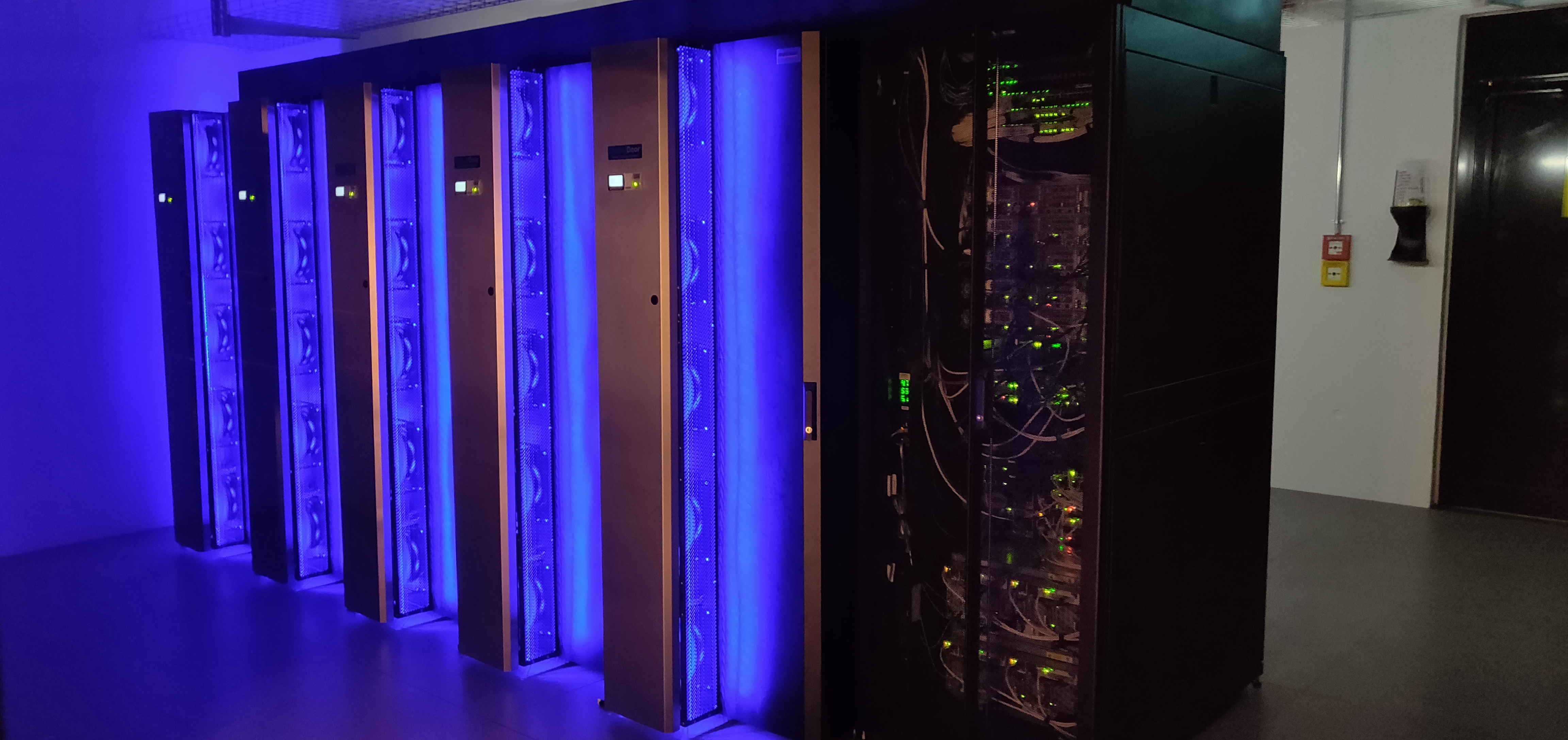
The Noctua system – the name is Latin for “Little Owl,” will be put into a shiny new datacenter that Paderborn and the federal Germany government and the state of North Rhine-Westphalia together kicking in €25.4 million (just under $30 million) to build that datacenter, purchase the Noctua machine, and run it for four years out through 2022. The Noctua system, which costs €10 million ($11.8 million) is based on the Cray CS 500 cluster design, and it will be comprised of 256 CPU compute nodes that each have a pair of Skylake Xeon SP-6148 Gold processors, which have a base frequency of 2.4 GHz with turbo up to 3.7 GHz and which have 20 cores each. The servers have 192 GB of main memory each. When you add up all of the cores, double precision floating point oomph, and memory, it comes to 10,240 cores with 535 teraflops and 48 TB in the aggregate. The whole shebang is linked together using Intel’s 100 Gb/sec Omni-Path 100 series. For storage, Paderborn University has chosen 720 TB of capacity on Cray’s ClusterStor L300N arrays, which are running the Lustre file system and which have the NXD flash accelerator embedded.
The prior Oculus – short for Owl Cluster – was a hybrid system with 551 “Sandy Bridge” Xeon E5 v1 servers with a total of 9,920 cores and 45 TB of main memory rated at 200 teraflops, plus 20 nodes with Intel Xeon Phi coprocessors that added another 40 teraflops and another 40 nodes with Nvidia Tesla K20X or GeForce GTX 1080 GPU accelerators that added a bunch more. This prior cluster was linked using 40 Gb/sec QDR InfiniBand networking from Mellanox Technology, and it had a homegrown 500 TB BeeGFS parallel file system. (BeeGFS was developed in Germany and was originally called the Fraunhofer Gesellschaft File System.)
In being hybrid, the Noctua machine is similar to Oculus, but in this case, there are no Xeon Phi or Nvidia accelerators, but just FPGAs. The Noctua machine has another 16 nodes in the CS 500 cluster that each have a pair of Intel Stratix 10 FPGAs in them. To be specific, the nodes are equipped with the 520N PCI-Express card made by Nallatech. This card has a 32 GB of DDR4 memory linked to the FPGA, which is an Intel Stratix 10 GX 2800.
“We have specifically selected an FPGA card with four 100 Gb/sec network ports, which will allow us to build a custom interconnection network between the FPGAs, either as a direct peer-to-peer topology – for example, a torus – as a switched network,” professor Christian Plessl, director of the Paderborn Center for Parallel Computing, tells The Next Platform.
At the moment, the Paderborn Center has six different FPGA systems that it has been doing research with, including an old Convey HC-1 system from 2010 and a Maxeler Technologies MPC-C system from 2012 to a bunch of X86 systems with FPGAs. The center got its hands on a Power8 system from IBM with FPGA cards from AlphaData back in 2016, and last year it installed an eight-node cluster wit two AlphaData FPGA cards per node to test out the ideas that are going to be put into production with Noctua. Interestingly, last year Paderborn University got a ten-node cluster, called Harp, based on that prototype “Broadwell” Xeon E5 processor and the Arria 10 FPGA from Intel on the same package, which was unveiled in March 2016. This hybrid prototype chip has been subsequently supplanted this past May by a production hybrid chip that mixes a 20-core Skylake Xeon SP-6138 with an Arria 10 GX 1150. The Xeon half burns at 125 watts and the FPGA half burns at 70 watts. It is interesting that Paderborn University did not put these production Xeon SP-6138P hybrid CPU-FPGA processors into the CS 500 nodes. Rather, it opted for standard nodes with PCI-Express accelerators, which consume 225 watts but which can operate independently from the CPUs.
The programming environment for a hybrid machine like the Noctua cluster is as interesting as the underlying hardware. “We use the Intel OpenCL SDK for FPGAs, and we think that this design flow provides the best productivity for developers with a computational science background,” explains Plessl. “Experts in FPGA development still have the ability to optimize the results using compiler directives or even integrate highly optimized arithmetic components implemented with a low-level hardware description language with the rest of the accelerator design.”
In theory, each of those Nallatech cards provides 10 teraflops of single precision floating point performance if you configure the gates for this kind of math. So that is another 320 teraflops at single precision on top of the 535 teraflops at double precision. But Plessl warns that the math is not that simple.
“Quantifying the additional compute delivered by the FPGAs is difficult because the achievable performance is by nature application specific,” says Plessl. “By just using all DSP blocks in every cycle, each FPGA can reach around 10 teraflops single precision peak performance. In practice, this is not the typical design point where FPGAs provide their key benefits. The sweet spots for FPGAs are application kernels that don’t come close to their nominal peak performance on CPUs due to problems when using vector units, or overheads with synchronization, irregular data accesses, or unconventional arithmetic operations.”
Paderborn University expects for the system to be up and running by the end of October, and presumably it will be moved to the new datacenter when it is completed next year. Believe it or not, this will apparently be the largest FPGA accelerated system in academia. Way back in the day, oil and gas giants were building experimental FPGA systems that were much larger, and so were some life sciences and financial services companies, but they abandoned these efforts for all-CPU systems. Now, the hybrid pendulum is swinging back for some classes of applications and customers.

AMD Roadmaps Lead To Mountains Of Money
IT organizations, especially the key hyperscalers and cloud builders, don’t buy point products, they buy roadmaps. And they pay for them, too. And the precise focus that AMD has brought to bear in its eight year turnaround has made it have the most credible and expansive CPU product line for …
Intel Hits Bottom In The Datacenter – Maybe
It would be hard to pick a worse time to not have an XPU offload engine that can do lots of matrix math at mixed precision and that can ship in volume. But this is precisely where Intel finds itself as there is a server recession in the datacenter. And …
Xilinx Tunes Up FPGAs For HPC, Graph Analytics
High performance computing hardware is really a software game, and the software we are referring to is at a very low level where deep expertise in libraries and solvers can make the difference between a capable device performing up to its specifications and, well, not so much. If you scan …
Be the first to comment