

This week we have heard much about the inference side of the deep learning workload, with a range of startups emerging at the AI Hardware Summit. These new architectures are taking aim at the big companies like Nvidia and Intel, challenging the power consumption and performance figures the growing cadre of datacenter and edge delivery on trained models.
The TPU has naturally emerged as a point of comparison, even if doing so is difficult given limited data about performance. But this week, Google has outlined the architecture of its TPU and talked for the first time about how they are considering inference with comparisons between GPUs and Haswell CPUs in particular.
When Google first deployed the first-generation TPU in its datacenters in 2015, deep learning was just falling into the mainstream gaze. At that time, the training side of the workload presented major challenges, but with its newest TPU, Google is trying to trim inference times and efficiency figures lower. The company says that their TPU has provided between 30X-80X performance and efficiency gains for important applications, including image recognition, natural language processing, and various other deep learning tasks, but this has been assumed to be for the most lengthy part of the process—training.
“Since transistors are not getting much better (reflecting the end of Moore’s Law), the peak power per mm2 of chip area is increasing (due to the end of Dennard scaling), but the power budget per chip is not increasing (due to electro-migration and mechanical and thermal limits), and chip designers have already played the multi-core card (which is limited by Amdahl’s Law), architects now widely believe the only path left for major improvements in performance-cost-energy is domain-specific architectures.”
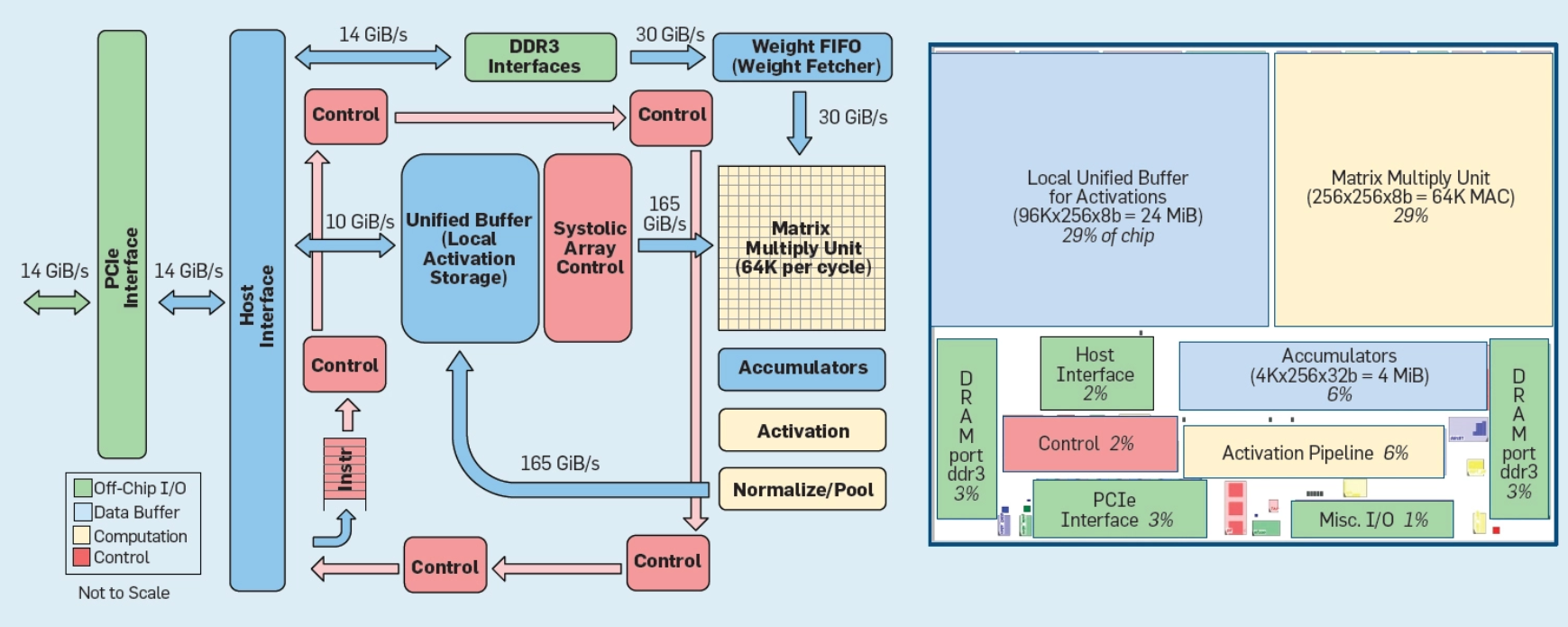
In their ACM work, the authors have provided a detailed architecture view below. The main computation is the yellow matrix multiply unit. Its inputs are the blue weight FIFO and the blue Unified Buffer, and its output are the blue accumulators. The yellow activation unit performs the nonlinear functions. The floor plan of the die on the right shows the blue memory is 35% and the computation is 35% with the green I/O as 10% and the red control just takng up 2% of the die. Google says the control is much larger and more difficult to design in a CPU or GPU.
One of the major points they address is that inference is actually efficient on the TPU. However, they note that datacenter inference do not need high throughput as much as fast performance. “We were surprised that Google TPU developers had strong response-time demands, as some suggested in 2014 that batch size would be large enough for the TPU to reach peak performance or that latency requirements would not be as tight,” the designers note.
“Google developers’ intuition was that if interactive services also wanted TPUs, most of them would just accumulate larger batches. Even the Google developers of one application in 2014 who cared about response time (LSTM1) said the limit was 10ms in 2014 but shrank it to 7ms when actually porting it to the TPU. The unexpected demand for TPUs by many such services, combined with the impact on and preference for quick response time, changed the equation, with application writers often opting for reduced latency over waiting for bigger batches to accumulate. Fortunately, the TPU has a simple and repeatable execution model to help meet the response-time targets of interactive services and such high peak throughput that even relatively small batch size results in higher performance than contemporary CPUs and GPUs.”
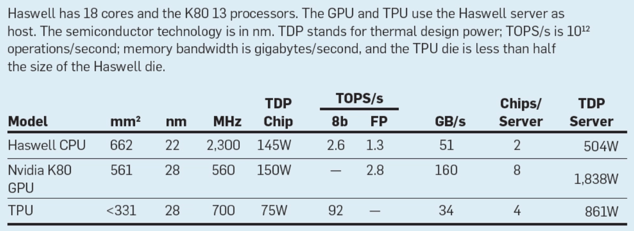
Not surprisingly, the authors also add the Nvidia K80s are not well-suited for inference. They say the TPU handles this better in terms of performance, energy, and cost.
“First, the TPU has only one processor, while the K80 has 13, and it is much easier to meet a rigid latency target with a single thread. Second, the TPU has one very large two-dimensional multiply unit, while the GPU has 13 smaller, one-dimensional multiply units. The matrix multiply intensity of DNNs fits arithmetic logic units arranged in a two-dimensional array. Third, a two-dimensional array also enables systolic implementation that improves energy efficiency by avoiding register accesses. Fourth, the TPU’s quantized applications use eight-bit integers, unsupported on the K80, rather than the GPU’s 32-bit floating point. The smaller data improves not only the energy efficiency of the computation, it quadruples the effective capacity of the weight FIFO and the effective bandwidth of the weight memory. (These applications are trained to deliver the same accuracy as floating point despite using only eight bits.) Fifth, the TPU omits features required for a GPU but unused by DNNs, thus shrinking the TPU chip, saving energy, and leaving room for other upgrades. The TPU chip is nearly half the size of the K80 and typically runs at one-third the power yet contains 3.5× as much memory. These five factors explain the TPU’s 30× advantage in energy and performance.”
While future CPUs and GPUs will surely run inference faster, a redesigned TPU using circa-2015 GPU memory would go three times faster and boost the performance/Watt advantage to nearly 70× over the K80 and 200× over Haswell.
We are still baffled about the choice of Nvidia’s K80 GPU as the point of comparison, especially for inference workloads. The K80’s place to shine is in training with its successors fitting the bill even better (Volta in particular). With Skylake available and no doubt available inside Google’s own datacenters it is also a wonder why Haswells are used. Nonetheless, when Google talks chip architecture, it’s our job to listen, even if the basis for comparing performance is off kilter.
Please take a look at the detailed ACM paper.

The Battle Begins For AI Inference Compute In The Datacenter
The major cloud builders and their hyperscaler brethren – in many cases, one company acts like both a cloud and a hyperscaler – have made their technology choices when it comes to deploying AI training platforms. They all use Nvidia datacenter GPUs and, if they have them, their own homegrown …

Feeding The Datacenter Inference Beast A Heavy Diet Of FPGAs
Any workload that has a complex dataflow with intricate data needs and a requirement for low latency should probably at least consider an FPGA for the job. FPGAs have, of course, been operating in the datacenter for three decades, usually under the skins of some appliance, but FPGAs are coming …
Further Funding Flows to Canadian AI Inference Hardware
AI inference hardware startup, Untether AI, has secured a fresh $125 million in funding to push its novel architecture into its first commercial customers in edge and datacenter environments. Intel Capital was a primary investor in Untether AI since its founding in 2018. When we did a deep dive on …
Be the first to comment