
At the GPU Technology Conference last week, we told you all about the new NVSwitch memory fabric interconnect that Nvidia has created to link multiple “Volta” GPUs together and that is at the heart of the DGX-2 system that the company has created to demonstrate its capabilities and to use on its internal Saturn V supercomputer at some point in the future.
Since the initial announcements, more details have been revealed by Nvidia about NVSwitch, including details of the chip itself and how it helps applications wring a lot more performance from the GPU accelerators.
Our first observation upon looking at the specs and the performance metrics that Nvidia has released is that clearly GPU compute is I/O bound as well as memory capacity and memory bandwidth bound. But the capacity has been addressed by getting the capacity on the Volta GPUs up to the 32 GB that we had expected when they were announced last year, and that, frankly, Nvidia had hoped to deliver with HBM2 stacks with the “Pascal” P100 accelerators two years ago. The 900 GB/sec of aggregate memory bandwidth that is delivered with the HBM2 on the Volta GPUs accelerators is pretty close to the 1 TB/sec that was expected originally from the Pascal roadmap. I/O bandwidth into the GPU complex and across it as nodes have scaled out with more and more GPUs, has been the issue. And NVSwitch does a good job of addressing this, and thereby boosting performance because those GPUs are kept busier and they can share data faster.
There are a lot of different topologies in which the NVSwitch could be deployed in a system, and clearly the design goal with the implementation employed in the DGX-2 system that Nvidia will start shipping in the third quarter and that will, we presume, be the first of many OEM and ODM systems that will make use of the GPU switch, is provide enough I/O bandwidth to make full use of that memory and compute capacity in any given size of GPU cluster within a fat node. And despite how we like to do though experiments about the possibilities of any new technology, we got the distinct impression from Ian Buck, vice president and general manager of accelerated computing at Nvidia, that NVSwitch would not be used to couple multiple nodes together, as is sometimes done with PCI-Express switches within one, two, or three racks of servers. That doesn’t mean ODMs and OEMs won’t try, and we are sure someone will be experimenting with this as soon as they can get their hands on NVSwitch silicon.
Speaking of which, we finally got a peek at the NVSwitch silicon, and here it is:
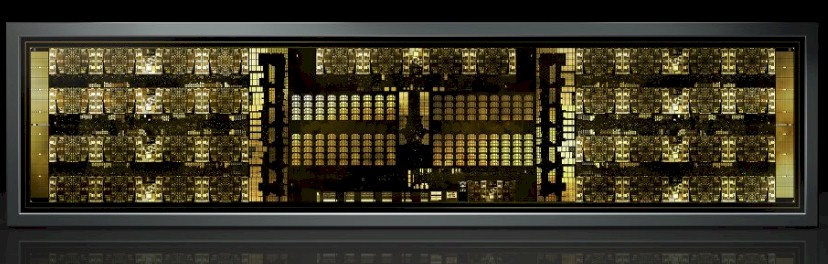
Those 2 billion transistors are etched using the same 12 nanometer FinFET process at Taiwan Semiconductor Manufacturing Corp that the Volta GPUs employ. This is a cutting edge and custom process that is ahead of the 14 nanometer node that is being used for other devices, including the prior generation “Pascal” GPUs that still dominate Nvidia’s volumes. We suspect that this process is being used for the NVSwitch ASICs, although Nvidia has not confirmed this.
Here are the parts of that NVSwitch chip, all blocked out:
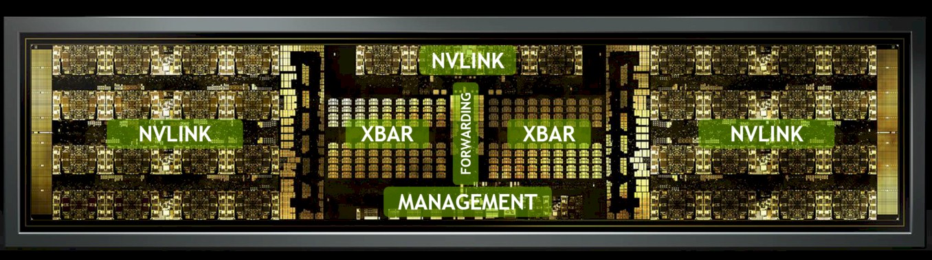
This is very interesting indeed. There are two blocks of eight NVLink ports, on the right and left side of the die, plus another two NVLink ports in the top center of the chip. The crossbar seems to link the eight ports on the right side in a non-blocking manner with the eight ports on the left, and in the dead center of the die are forwarding circuits that we presume are used to link either set of NVLink port bundles with the two NVLink ports at the top. This is a different configuration than we think was intimated before this die shot came out and that was suggested by this diagram that was put out on announcement day last week:
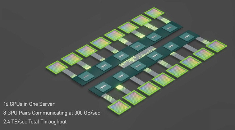
You can’t really tell what is going on inside the NVSwitch ASICs or between them, but if you squint you can see six NVLink ports coming out of each GPU into the NVSwitch fabric. Each NVLink port has eight lanes that run at 25 Gb/sec each way to get that 50 GB/sec of aggregate bidirectional bandwidth per port, and the NVSwitch topology used in the DGX-2 system gangs up all six ports on each Volta GPU to provide 300 GB/sec of aggregate bidirectional bandwidth between the GPUs and the GPU memory fabric (150 GB/sec each way).
When this story first ran, we did a little though experiment, to try to guess what was going on itside of this switch fabric because Nvidia was not yet ready to talk about its architecture. When we looked at that chart and knew that each NVSwitch had 18 ports and that there were 16 GPUs being connected, we assumed at all of the ports on the NVSwitch were being used. We surmised that this might not be the case, leaving room for expansion in the future. There are 96 downlink ports that are necessary to link to the 16 GPUs, at six ports per GPU. That left another 120 ports that we presumed were used for the cross-interconnect between the two halves of the GPU compute complex. This may not have been a valid assumption, or at least it presents some interesting ways of linking lots of GPUs and switch chips together.
We went back into the keynote presentation of Jensen Huang, Nvidia co-founder and chief executive officer, and scraped this image off the wall:
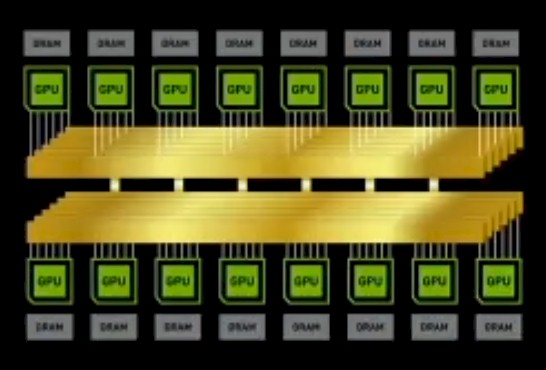
This chart shows that each GPU has one NVLink port hooked into each of the six NVSwitch chips used on each side of the GPU complex in the DGX-2. Hanging eight GPUs off the cluster of six NVSwitch chips would eat one port on each side of the NVSwitch chip, if this diagram is representative. That leaves another eight downlink ports on the NVSwitch chip completely untouched, if we were right. That would mean that the first iteration of NVSwitch could actually tightly couple up to 32 GPUs in a single system rather than the 16 GPUs shown in DGX-2.
This implied that the aggregate bandwidth across those eight GPUs in each half is 2.4 TB/sec, just as Nvidia has said, but that there is also another 2.4 TB/sec there to use in the future – provide the NVlink backplane can expand enough in a system to span four enclosures instead of two. This may not have been be possible with the current DGX-2 backplane, which might explain why Nvidia did not push NVSwitch to the hilt. If this is indeed the case.
Based on these chip shots and diagrams, we thought that the two NVLink ports shown in the center top of the die are uplinks to the fabric. We assumed, not knowing the topology of the fabric hooking the two halves of the GPU complex together, that the remaining 120 ports were providing 6 TB/sec of aggregate bandwidth across the two halves. This seems unlikely if those two ports are the only uplinks between the two layers of the GPU memory network. The DGX-2 topology that Huang showed has six fat pipes linking the two halves together. We don’t think this interconnect here is an all-to-all topology across the switch chips because that would require an additional 11 ports of NVLink; if we are right about how the GPUs link to the chip, there are only ten ports left over – eight port on one of the two NVLink blocks and two in the center that we have been calling uplinks.
Leaving GTC18, we honestly didn’t know what the interconnect topology was between the two sets of NVSwitches – and no one else did outside of Nvidia and its key partners, either. Anything we could diagram on graph paper had a lot of hops between the switches or needs more ports on the uplinks.
We thought a two-way ring was pretty, but there could be six hops between switch chips in a worse case scenario (half way around the ring in either direction). What we do know is that Nvidia did say it was a “fully connected crossbar internally” on the NVSwitch but never said that it was fully connected, all-to-all communication across the two halves of the virtual GPU brain. As long as the data can be partitioned across the GPUs, and accesses are not huge across those halves, it is no worse than having regular NVLinks between CPUs and GPUs. We like the answer that there is a ring interconnection going two ways between the switch chips and there is room for more GPUs. This is a much more fun answer than all of the ports are already used up.
If you took this chart above literally, then the two NVLink uplink ports coming out of one NVSwitch could be cross-coupled directly to the uplinks on another NVSwitch, just like you can do with Tesla accelerators or even with a pair of Quadro cards with NVLink using a bridge. But that would mean only pairs of GPU switches were linked across the GPU compute complex and some other mechanism (such as the PCI-Express network) would be needed to jump across all of the switches. This didn’t make sense to us.
The other option is that the crossbar is distributed. The bottom part of the crossbar is used to link the eight GPUs to each other in each half and then the upper part is a distributed crossbar, with a piece residing in each switch, that links the switch side of that crossbar to each other using a direct link between the switch chips. Each switch chip is hooked to each GPU on each side, so with an extra hop, any GPU can route out and hit any other GPU. The bandwidth between the switches is the same as between the GPUs, at 50 GB/sec, and twelve of the GPUs could talk across the crossbar bridge between the halves at a time.
Nvidia could have just had one NVSwitch and hung all of the 16 GPUs off of it, and used the other two uplinks for a higher level network or to link to a Power9 chip, which has native NVLink ports. This would be a much lower bandwidth setup, obviously. And there would not be as many paths between the GPUs, which could result in contention on the memory fabric.
After all this conjecture, we said that we hoped Nvidia would divulge some more details on the NVSwitch setup in the DGX-2 as well as possible other topologies we might see from OEMs and ODMs. As we said before, this switch was the neat bit announced at GTC18. And after this story ran, Denis Foley, senior director of architecture at Nvidia and one of the architects of the NVSwitch chip, reached out and said that we were overthinking it, and the thing that got us off course from how it actually works is that those two uplink ports are not actually used in the DGX-2. But we still say they could be used in precisely the fashion we outlined above, in some future product either from Nvidia or from an ODM or OEM.
So, here is how the fabric actually works as implemented in the DGX-2. As we surmised, eight Volta SXM3 GPUs hang off of one half of the NVLink downlink ports on half of the NVSwitch chip. Flip a mirror image on another NVSwitch chip and hang eight more GPUs off of it with one downlink each. That leaves the other eight downlinks on the inside halves of the pair of NVSwitches, and you plug the two switches together that way. (Why you cannot do this with just one switch chip is not entirely clear.) Now, do that five more times and overlay those six crossovers and then gang up the NVLink ports coming out of the GPUs and also gang up the ports between the switch chips to boost the aggregate bandwidth by a factor of 6X, from 50 GB/sec to 300 GB/sec. It takes two hops therefore to go from a GPU to another GPU on the half (one hop up to the switch chip and one hop back down to the other GPU) and three hops to go from one GPU enclosure to the other across the GPU backplane (one hop from the GPU up to the switch chip, another hop to the adjacent switch chip, and one last hop down to the GPU.)
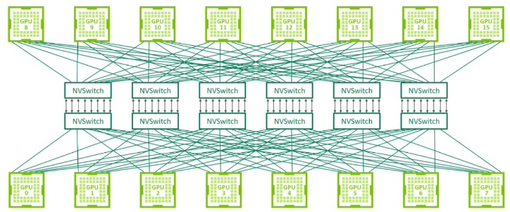
It is simpler than we thought, but that doesn’t mean these other scenarios will not – or cannot – be used. We think the NVSwitches are laid down in this manner, in pairs, to allow more sophisticated topologies because it is seems obvious from this that you only need six NVSwitches to link together 16 GPUs, but by having a dozen chips, you have twice as many ports across which to cross-link any GPU to any other. What is also immediately obvious is that the NVSwitch provides some very high bandwidth between the GPUs and this has a very dramatic effect on performance.
To show the effect of NVSwitch, Nvidia pit a pair of its DGX-1 servers, each with eight Volta V100s and connected by four 100 Gb/sec InfiniBand ports to each other against DGX-2 with 16 of the Volta V100s. We presume, because Nvidia did not specify, that all three machines were equipped with the 32 GB memory SXM3 variants of the Volta V100 accelerators and that the old DGX-1s were not using the 16 GB SXM2 versions of Volta. By doing it this way, the tests that Nvidia ran would show off just the benefit of the NVSwitch inside the DGX-2 compared to NVLink inside of the DGX-1s and InfiniBand across them. Here is what the results of the tests look like:
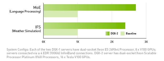
The top benchmark shows the results for the Mixture of Experts, a neural network used for natural language processing developed by Google and running atop the TensorFlow framework. There is a significant amount of all to all communication in this cluster of 128 different neural networks, which each have their own domain expertise. This test exercised the Tensor Core units on the Volta, and it looks like Google ran these tests itself and therefore had early access to DGX-2 machines. The DGX-2 had 2.7X the performance of the pair of DGX-1s on this test.
In the traditional HPC realm, Nvidia tested the Integrated Forecasting System (IFS) global weather forecasting system from ECWMF in the United Kingdom. This is not the full weather model, but a chunk that focuses on spherical harmonics transformation that really stresses the GPUs and is a very heavy part of the full IFS application. In this case, for this portion of the code, the speedup of DGX-2 over the pair of DGX-1s is 2.4X. (It would have been interesting to see CPU-only comparisons for both of these tests.)
It is interesting to contemplate what would happen if there were more GPUs in a fat node, either by thinning out the network with a different topology or by adding more NVSwitch chips . There is probably a point of diminishing returns, just as there are for NUMA clusters in CPU-only shared memory systems. The biggest practical NUMA machines had 128 sockets, and really, after 32 sockets the queuing and latencies get pretty hairy. Which is why we don’t see them anymore.


HPC In 2020: AI Is No Longer An Experiment
If we could sum up the near-term future of high performance computing in a single phrase, it would be more of the same and then some. Although no “revolution” is in the horizon, the four major trends of the past decade – the expansion of artificial intelligence technology, processor diversification, …
Building A Hassle-Free Way To Port CUDA Code To AMD GPUs
Emulation is not just the sincerest form of flattery. It is also how you jump start the adoption of a new compute engine or move an entire software stack from one platform to another with a different architecture. Emulation always involves some form of performance hit, but if you are …
Nvidia’s Grace-Hopper Hybrid Systems Bring Huge Memory To Bear
If you were hoping to get your hands on one of Nvidia’s “Grace” Arm-based CPUs, then you better be prepared to buy a pretty big machine. The Grace-Grace superchips, which have two CPUs on a package with NVLink 4.0 chip-to-chip (C2C) links, and the alternative Grace-Hopper GH200 superchips that weld …
So in theory, this NVSwitch can allow a DGX box with 3TB of DDR4, 4 Xeons and 32 V100s with a total of 1TB HBM2, with all the GPUs in the system communicating over the NVSwitch fabric through a bigger backplane? All with a one hop within an 8 GPU board and still with a maximum of 3 hops to anywhere within that system?
The chosen topology allows the backplane connection to be passive. While they could connect all GPUs with 6 switch chips, this would either require that the backplane to be active, containing the switch chips(which has cost issues, real estate issues, and cooling issues), or for half the traces to go through 4 connectors/sockets along with the backplane trace likely resulting in unacceptable S/N margin (and also require 2 different GPU motherboard types).
So by doing it with the mirrored topology, they not only get symmetrical motherboards but a passive backplane and the switch chips also effectively do double duty as electrical repeaters. In addition, if they want to in the future, it allows future further designs with a double sided backplane supporting an additional layer of switch boards to support a larger topology.