

There are two supercomputers named “Aurora” that are affiliated with Argonne National Laboratory – the one that was supposed to be built this year and the one that for a short time last year was known as “A21,” that will be built in 2021, and that will be the first exascale system built in the United States.
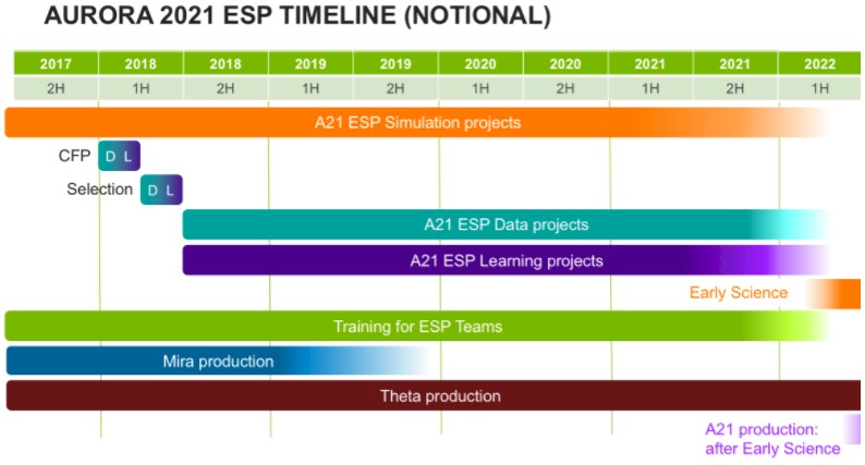
Details have just emerged on the second, and now only important, Aurora system, thanks to Argonne opening up proposals for the early science program that lets researchers put code on the supercomputer for three months before it starts its production work. The proposal provides a glimpse into what the second Aurora machine might look like, and it bears some similarities to the Aurora machine that Intel and Cray had expected to put into the lab this year.
The new information comes in the wake of Oak Ridge National Laboratory and Lawrence Livermore National Laboratory providing a timeline for their respective “Frontier” and “El Capitan” exascale supercomputers. It looks like Frontier is coming in early 2022, with El Capitan following later in the year. Their architecture has not yet been revealed, but it is excepted that both Oak Ridge and Lawrence Livermore will stick with hybrid CPU-GPU systems and that they will be comprised of IBM’s Power10 processors and some as-yet-unrevealed future Nvidia GPU accelerator. But no one has made any promises in this regard.
The original Aurora machine was to be designed by Intel and Cray, using the now defunct “Knights Hill” Xeon Phi many core processor and the still expected 200 Gb/sec Omni-Path 200 interconnect, both from Intel. The system was going to be based on Cray’s future “Shasta” system design, and the Omni-Path interconnect was to be bolstered with a healthy dose of the technology underpinning Cray’s “Aries” Dragonfly interconnect. (Intel actually bought Cray’s interconnect business back in 2013 just for this purpose.) That original Aurora design was to have 7 PB of on-package, high bandwidth memory with an aggregate of more than 30 PB/sec of bandwidth across the more than 50,000 nodes in the system. The Omni-Path 200 links were to be on the Xeon Phi package, delivering 2.5 PB/sec of aggregate node link bandwidth and more than 500 TB/sec of interconnect bisection bandwidth.
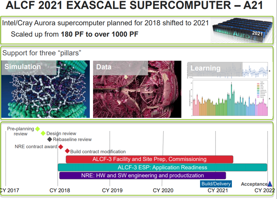
Flash forward to the new and improved Aurora, and we now know that it will also have around 50,000 nodes and over 5 PB of various kinds of memory when installation begins in late 2020 and into early 2021, with acceptance slated for early 2022. (Those feeds and speeds are the new bit.) The nodes will be equipped with high bandwidth memory, and we suspect that Intel will be using the same HBM-style memory deployed on GPU accelerators, not the MCDRAM memory that it created with Micron Technology and that it had used in the “Knights Landing” Xeon Phi 7000 series of accelerators and standalone processors.
As you can see, the node count is roughly the same between the two different versions of the Aurora machine, but the amount of compute, presumably expressed in double precision floating point math as is the tradition in the HPC world, has gone up by a factor of at least 5.5X from the 180 petaflops expected with the original Aurora (let’s call it A18 so we have a name for it) to the 1,000-plus petaflops of the A21 system that Intel and Cray are building for Argonne. The memory footprint on the A21 machine is actually smaller, by 30 percent, which seems like an odd choice unless the memory is unified in a way that makes it more coherent across serial and parallel compute elements. This is precisely what we expect on the compute front, and Lawrence Berkeley National Laboratory has provided some thoughts about the future of accelerated computing that leads us to believe that the future NERSC-10 exascale machine will be based on the same kind of compute, albeit possibly a follow-on generation giving its timing.
Here in italics is what Argonne has told researchers who are bidding to run jobs on the future A21 machine, which provides some insight into the architecture:
- Nodes will have both high single thread core performance and the ability to get exceptional performance when there is concurrency of modest scale in the code.
- The architecture is optimized to support codes with sections of fine grain concurrency (~100 lines of code in a FOR loop for example) separated by serial section of code. The degree of fine grain concurrency (number of iterations of loop for example) that will be needed to fully exploit the performance opportunities is moderate. In the ~1000 range for most applications.
- Independence of these loops is ideal but not required for correctness although dependencies that restrict the number of things that can be done in parallel will likely impact performance.
- There is no limit on the number of such loops and the overhead of starting and ending loops is very low.
- Serial code (within an MPI rank) will execute very efficiency and the ratio of the performance of the serial to parallel capabilities is a moderate ratio of around 10X, allowing for code that has not been entirely reworked to still perform well.
- OpenMP 5 will likely contain the constructs necessary to guide the compiler to get optimal performance.
- The compute performance of the nodes will raise in a manner similar to the memory bandwidth so the ratio of memory BW to compute performance will not be significantly different than systems were a few years ago. A bit better in fact than they have been recently.
- The memory capacity will not grow as fast as the compute performance so getting more performance through concurrency from the same capacity will be a key strategy to exploit the future architectures. While this capacity is not growing fast compared to current machines it will have the characteristic that the memory will all be high performance alleviating some of the concerns of managing multiple levels of memory and data movement explicitly.
- The memory in a node will be coherent and all compute will be first class citizens and will have equal access to all resources, memory and fabric etc.
- The fabric BW will be increasing similar to the compute performance for local communication patterns although global communication bandwidth will likely to not increase as fast as compute performance.
Like everyone else, we have been trying to puzzle out what Intel would propose on the compute front, and NERSC at Lawrence Berkeley has provided some insight which we think is relevant for Argonne as well. This architectural block diagram from its March 2016 update on the “Edison” NERSC-7, “Cori” NERSC-8, and future NERSC-9 and NERSC-10 machines tells the story we think will play out:
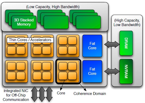
Such a proposed chip coming from Intel would essentially be a Knights family massively parallel processor mixed with some Xeon cores on the die to boost serial performance for selected sections of the code. It would, in effect, be a mixing down on the die of the kind of hybrid Xeon-Xeon Phi systems that many of the world’s largest HPC centers have installed – most Xeon Phi systems have a heavy Xeon component for backwards compatibility with code that is more compute intensive than can be handled.
This design should be no surprise whatsoever, and it is a wonder why Intel is being so cagey about the plan for the A21 implementation of Aurora. It suits no purpose, particularly when everyone knows that it had to rejigger the Aurora contract because whatever it was doing with the canceled “Knights Hill” processor for the original A18 machine was no longer going to suit the market. You can blame machine learning for that, we think. These massive machines have to be good at both traditional simulation and modeling in the HPC realm as well as for machine learning and various kinds of data analytics.
This processor design is familiar in HPC systems, and in fact, looks a bit like IBM’s Power-based “Cell” processor, used in the first petascale system, “Roadrunner,” installed at Los Alamos National Laboratory between 2006 and 2008 and decommissioned in 2013. The original PowerXCell8i processor used in Roadrunner had a single Power4 core and eight “synergistic coprocessors” that were parallel computing units suitable for doing either math or graphics processing, While Roadrunner hung six of these processors off a pair of AMD Opteron processors across four blades, the Cell chips were designed so they could be a primary, standalone compute element, and were often used as such in other devices. IBM had four generations of Cell chips, culminating with a variant with two fat processor cores and 32 of the coprocessors on a die, which never saw the light of day and which, frankly, opened the door for Nvidia to walk through with its GPU offload model on hybrid CPU-GPU systems.
This fat core-skinny core hybrid approach is also used in the SW26010 processor deployed in the Sunway TaihuLight supercomputer which was developed at the National Research Center of Parallel Computer Engineering and Technology (NRCPC) and is in full production running early-stage workloads at the National Supercomputing Center in Wuxi, China. In that design, there is one fat core and four auxiliary meshes of skinny cores, each with 64 cores, for a total of 260 cores.
It is not hard to conjecture that the Aurora A21 machine will be a hybrid of Xeon fat cores and skinny Atom cores with incredibly juiced AVX math units. Frankly, there is no better choice for Intel to make, since there is no one CPU that can do it all.

For HPC Cloud, The Underlying Hardware Will Always Matter
Decades of cloud collaborations and optimizations have brought solid performance and cost efficiencies to cloud. Those who require high performance computing (HPC) resources tend to set their own rules when it comes to systems. Highly tuned for blazing fast computation and communication with software stacks optimized to match, these users …

The Killer Apps For FPGAs Could Be SmartNICs And Storage
If FPGAs are going to take off in the datacenter in their own right, they are going to need their own killer apps. Plural. At The Next FPGA Platform event that we hosted recently in San Jose, there was plenty of talk about how FPGAs have been embedded in all …
The Expanding CXL Memory Hierarchy Is Inevitable – And Good Enough
The Hot Chips 34 conference that is normally held at Stanford University is in full swing this week, and thanks to the coronavirus pandemic is being held entirely online. Which means we have to buy our own ice cream and make our own lunches as we ponder the presentations offered …
If Intel does indeed go with fat and skinny cores, that sounds like it will be the x86 equivalent of the Nvidia MCM GPU plus host processor likely to be in El Capitan and Frontier or the big.LITTLE style ARM V8 cores in Post K. In which case, the true exascale systems are starting to get more similar.
I do wonder if Intel will follow Nvidia in adding some kind of machine learning specifc cores to whatever processor Aurora A21 uses.
It’ll also be very interesting how that the 5PB of memory breaks down into in terms of DRAM and nonvolatile memory. Same goes for the other exascale systems with DRAM being so expensive.