It is going to be a busy week for chip maker Qualcomm as it formally jumps from smartphones to servers with its new “Amberwing” Centriq 2400 Arm server processor during the same week that it has received an unsolicited $130 billion takeover offer from sometimes rival chipmaker Broadcom.
The Centriq 2400 is the culmination of over four years of work and investment, which according to the experts in the semiconductor industry we have talked to, easily took on the order of $100 million to $125 million to make happen – remember there was a prototype as well as the first generation Amberwing chip – and probably several hundred chip engineers to design. And now, there is another credible Arm server processor in the datacenter fray alongside the ThunderX and ThunderX-2 from Cavium and the X-Gene 1 and X-Gene 2 from Applied Micro. It could turn out that, based on the feeds, speeds, pricing, and substantial financial heft of Qualcomm that the Centriq 2400 rises to the top of the Arm server pack in relatively short order – particularly with the top brass at Microsoft’s Azure public cloud business standing up and committing to deploying the Amberwing chip in its development cloud and making the Arm instruction set a peer to the X86 processor for application development.
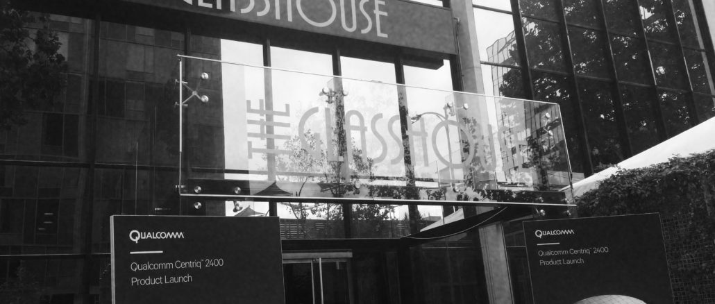
Microsoft is the most vocal among the hyperscalers to admit that it wants to have an alternative to the X86 architecture for its cloud, and Google has been pretty vocal in its support of IBM’s Power9 chip through the establishment of the OpenPower Foundation. The search engine giant is also rumored to be the big hyperscaler that reached out to Qualcomm many years ago with an investment to encourage the chip maker to go for it. Qualcomm did not divulge its plans to assault the glass house – which is why that feature image at the top, showing where the Amberwing launch event was hosted in San Jose, is funny as well as prophetic – until November 2014. That seems like a long time ago, but it generally takes three years to get a chip out the door from whiteboard to wafer. We presume at that time that the prototype Centric 1200, as it might have been called had it been formally launched, was shown in October 2015 that the plan had been to roll out this 24-core Arm chip but it was not impressive enough to beat the Intel Xeons of the time. All we ever knew about this chip is that it was based on a custom 64-bit core that was ARMv8-compliant, and everyone presumes that it was a variant of the “Kryo” core used in the Snapdragon 820 processors for mobile devices that had been beefed up with a lot more cores, plus more caches and more main memory to balance it all out.
Now the Amberwing is finally out of the bag and we can talk about what it is and then get on with the task of seeing how it stacks up to the other Arm chips, X86 chips, and Power chips in the market. Let’s start with the feeds and speeds.
Historically, Qualcomm has used either Samsung or Taiwan Semiconductor Manufacturing Corp as its chip manufacturing partners, so we figured one of these two would get the gig. The word on the street for the past two years has been that TSMC would get the job, but as it turns out it is Samsung with its 10LPE 10 nanometer chip processes that got the gig. As Qualcomm has contended many times – and as we have discussed previously – the PC chip, mostly made by Intel these days but with a smattering of chips from AMD, is no longer the volume leader among device chips and it is also not on the bleeding edge of process technology, either.
The two are related, and in an ideal situation, you want the highest volume chips to be on the latest processing nodes because this is the fastest way to perfect the manufacturing processes and therefore drive down the costs of that process so bigger, fatter, juicier chips can eventually be etched with them. These days, the chips used in smartphones are smaller than PC chips and they are in a lot higher volume, too, which means yields are generally better because of the relative size of the chips, and because of the volumes, you can ramp the new process relatively faster. The 14 nanometer node, back in 2014 when Qualcomm committed publicly to entering the server fray, was the last time that PC processors were out ahead of smartphone chips, and with the 10 nanometer node, which Qualcomm has jumped out first with its Snapdragon 850 chip earlier this year, it is keeping the Centriq 2400 pretty close behind it in the wake. Intel is having real troubles ramping up 10 nanometer processes for PC chips, and while it has promised to get Xeon server chips and Core PC chips at process parity, this may prove harder to do than it expects, and probably more costly.
In any event, the upshot of all of this is that Qualcomm, working with Samsung, is the first to market with a server chip etched in 10 nanometer processes, and that chip is based on an Arm architecture, and that is an accomplishment that will not go unnoticed by the datacenters of the world.
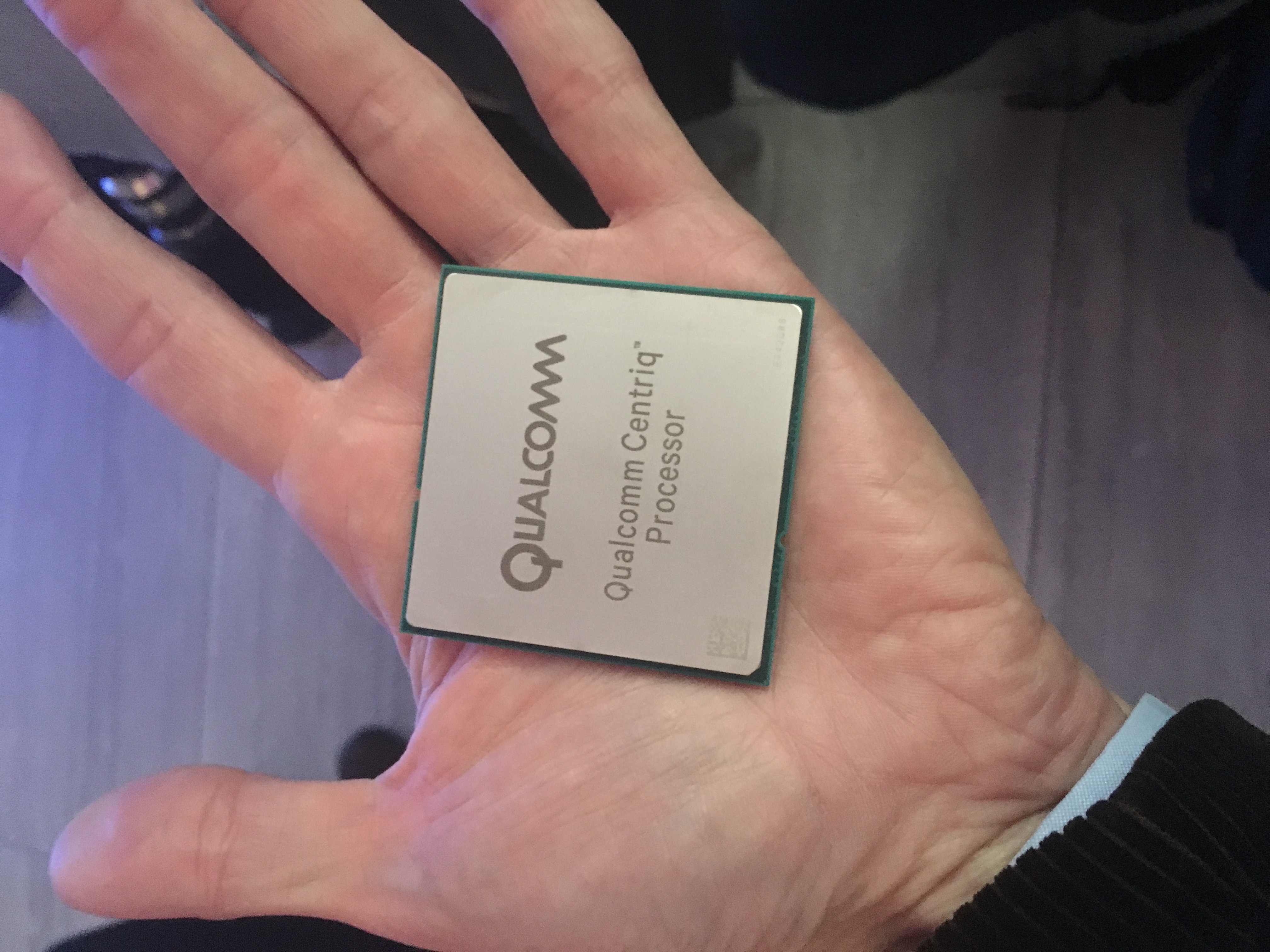
Back in August, at the Hot Chips conference in Silicon Valley, Qualcomm engineers revealed some of feeds and speeds of the Amberwing processors, but a lot of details were missing. Now we can fill in some of the blanks. First of all, the chip has over 18 billion transistors, which is a lot, and crams them all into a relatively small 398 square millimeters of space; the chip package weighs in at 55 millimeters by 55 millimeters, and looks about the same size as the original and unnamed Centriq prototype chip from two years ago.
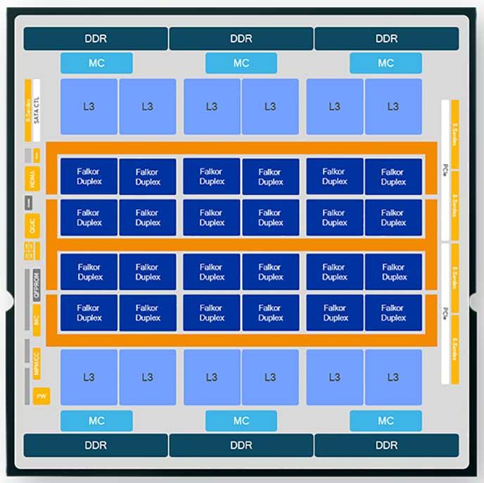
The Centriq 2400 starts with a chiplet based on a pair of “Falkor” 64-bit cores, which have a peak turbo frequency of 2.6 GHz as it turns out and a base clock speed of 2.2 GHz. The Falkor core is the fifth homegrown ARM core created by Qualcomm, which used non-custom cores licensed from Arm before that. The neat thing is that the Centriq 2400 only supports 64-bit processing as specified by the AArch64 spec from Arm Holdings, the chip division of SoftBank. The 32-bit AArch32 processing capability was stripped out of the Falkor core, and that little bit of extra transistors made some room for more cores on the die than might have otherwise been possible. Most server workloads these days are running in 64-bit mode on Linux, and even Windows Server 2016 is mostly 64-bit code, so this is not a big deal. The Falkor core does not implement simultaneous multithreading, so each core is its own thread and that is all you get.
We discussed the caching the caching mechanisms, which were borrowed from the mobile processors to boost their energy efficiency, last August, but we did not know about the cache sizes. The L0 cache that sits right next to the core and that can be reached without a clock cycle hit for super-fast access weighs in at 24 KB, with the L1 instruction cache coming in at 64 KB. Each of the 24 Falkor duplexes have a 512 KB L2 cache, and the L3 cache is broken into a dozen segments of 5 MB each, adding up to a 60 MB cache all linked using bi-directional, multiple ring coherent interconnect that also glues to cores together. That ring has more than 256 GB/sec of aggregate bandwidth – about a quarter of the Power9 chip, but still a lot. This ring interconnect is called the Qualcomm System Bus. It consists of two rings that wrap around a dozen core pairs each. The rings run at 2 GHz and have 64 GB/sec of bandwidth each way for that 256 GB/sec of bandwidth. The rings have even and odd interleaving as well as clockwise and counter-clockwise directions, and it will be interesting to see when and if Qualcomm switches to a mesh interconnect after running out of gas on the ring concept as Intel did with the Skylake Xeons.
The Amberwing chip has six memory controllers that support DDR4 memory running at up to 2.67 GHz and up to 768 GB of capacity, presumably using 64 GB memory sticks and hanging two sticks off each controller. Those six memory controllers deliver 128 GB/sec of aggregate peak bandwidth into and out of the main memory, and the memory controllers sport inline memory compression, which can push the bandwidth up even higher with decent compression ratios. The Amberwing chip has six PCI-Express 3.0 controllers on the die with a total of 32 lanes of I/O, which can be diced and sliced in a number of ways.
What the Amberwing chip does not have is integrate NUMA electronics to scale up the processing, memory, and I/O in a single system image. For a lot of the workloads that Qualcomm is targeting in the public cloud and for hyperscalers, a beefy single-socket machine is perfectly fine because anywhere from 10,000 to 50,000 nodes are ganged up to take on jobs anyway. AMD is making the same argument with it Epyq X86 server processors – that a single beefy socket can replace the typical two-socket Xeon server, which does not use anything close to a top-bin part with lots of cores anyway – and it is a convincing one that should worry Intel, which did not really launch a “Skylake” Xeon part tailored for single socket servers. (We suspect it will before too long.)
Speaking of Skylake, there are 51 different flavors of the chip, which you can see here, but there are only three different Centriq 2400 processors. The SKU list is so simple it almost doesn’t seem real, and while you might be thinking that Qualcomm could and should do versions that have fewer cores and lower prices to squeeze even more money from the bins. But for whatever reason, Anand Chandrasekher, senior vice president and general manager at Qualcomm Datacenter Technologies, who spearheaded the development of the Centriq chip, says that there will be no more SKUs for this Amberwing generation. Chandrasekher adds that Qualcomm is looking at such derivatives as it develops its next-generation “Saphira” cores for servers and the “Firetail” chips that will use them. It is possible that there could be NUMA electronics in these future chips, but it is equally likely, we think, that Qualcomm would try to employ software-based NUMA functionality like that from TidalScale, which we covered recently here.
In any event, here are the three Amerwing Centriq 2400 SKUs:
The naming convention seems to be meaningless, but it does suggest that if Qualcomm decided to offer different variants of the Centriq 2400, it could do that. It must have a pretty good reason for not doing it, because it is not like you can recycle partially dud chips as if they were made of metal, precious or otherwise. Clearly, the value of selling a Centriq with 12 or 24 cores would be higher than any scrap silicon value if it could be recycled. At these prices, it might cost $250 to buy a 12-core Centriq 2400 and maybe $500 to buy a 24-core version, and that might find some uses in storage. It is a peculiar choice to only have three SKUs when six or eight might cover the market better and increase the effective yields of the chip.
The Centriq 2400 chip has shipped to over a thousand sample chips to more than a dozen prospective customers, who are in various degrees of trial and proof of concept.
“It varies by customer,” says Chandrasekher. “Most customers are in some phase of testing leading to deployment. We expect production deployments to happen over the next twelve months, with some happening early in that cycle, some in the middle, and some later. But they are running real workloads, not test workloads. We are beyond that point.”
It certainly helps that SUSE Linux 12, Red Hat Enterprise Linux 7 and its CentOS 7 clone as well as the latest Ubuntu Server from Canonical are all supported, and Microsoft is working on a port of Windows Server 2016 for internal use on the Azure cloud for the chip, too, as it announced earlier this year. Rest assured that if companies ask for a commercial grade Windows Server 2016 for Arm chips, Microsoft will provide it and a minimalist stack, too.
In a follow-on story, we will take a look at how Qualcomm stacks up the Centriq 2400s against the new Skylake Xeons SP processors from Intel and its rivals in the Arm server chip space. This is getting interesting. Finally.


Great.
Now I want an Amberwing desktop…