

There is no question any longer that flash memory has found its place – in fact, many places – in the datacenter, even though the debate is still raging about when or if solid state memory will eventually replace disk drives in all datacenters of the world.
Sometime between tomorrow and never is a good guess.
Flash is still a hot commodity, so much so that the slower-than-expected transition to 3D NAND has caused a shortage in supply that is driving up the price of enterprise-grade flash – unfortunately at the same time that memory makers are having trouble cranking out enough DDR4 memory to meet demand. This is causing a temporary spike in server and storage prices, which have hurt the margins of ODMs and OEMs alike, but it has been great news for the semiconductor makers who etch flash and DRAM for a living. It is not a coincidence that Samsung has surpassed Intel as the world’s largest chip maker in the most recent quarter. Flash prices jumped around 50 percent and DRAM prices doubled over the past year, and that was just in time for the “Skylake” Xeon processor launch. While Intel’s Data Center Group revenues were up in the most recent quarter, we think they would have been even higher if the Skylake processors launched last fall or earlier in the spring and if flash and DRAM prices were not so high. The major server OEMs certainly felt the flash and DRAM price hikes pinch their profits, and complained each in their turn to Wall Street.
The consensus among the industry analysts at the Flash Memory Summit, which is being hosted in Silicon Valley this week, was that prices for DRAM and flash were expected to fall in the coming quarters, but not immediately. Howard Marks, chief scientist at Deep Storage, doesn’t expect for prices on these two memories to soften until late 2018 or early 2019, and reminds everyone that one of the issues is that the people who make DRAM also make flash and even though they can make both on many of the same fabrication lines, there are limits and even if they did boost production of one, they would have to lose production of the other. As long as everyone is experiencing the shortage, we think the industry is content to blame it on demand and rake in the bucks.
Jim Handy over at Objective Analysis gave an interesting presentation at the summit, and showed off how past shortages due to technological issues caused spikes in pricing on DRAM main memory, and that we should expect for these things to happen with all memory technologies because transitions are hard. Look at the curves since the 1990s on DRAM:
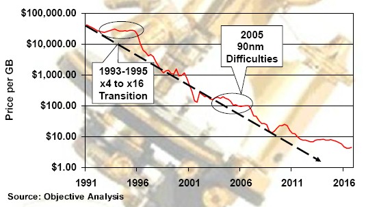
The interesting bit to us – and the one that is breaking apart the storage hierarchy in systems and across clusters, is how the price per GB for main memory is nowhere near the kind of Moore’s Law curve these machines require to keep the compute-storage-networking of systems on balance. Somewhere around the Great Recession, when server virtualization and multicore processing took off, the main memory that would have really made it more useful stopped getting less expensive. And in the past year, at the wholesale and street level, it has gotten significantly more expensive.
While flash and soon 3D XPoint will help alleviate pressure on main memory because they allow for more data to be more closely coupled with servers, flash is also having a price spike because of transitions from 2D planar to 3D stacked layouts as demand itself is on the rise, and when high demand hits constrained supply, it is never a good scenario for buyers or sellers. Here is what flash pricing on the spot and contract markets look like, according to Handy:

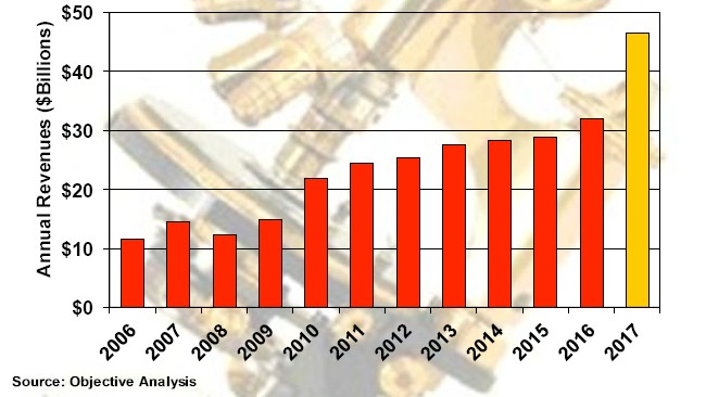
This curve is an average for all kinds of NAND flash, remember, and so is the aggregate revenues over time for NAND flash that Handy put together here:
What the industry wants is steady and growing demand and steady and growing supply with increasing manufacturing efficiencies, which is true of all semiconductor manufacturers, because this is what drives steady profits and prices for a chip come down. This demand spike and supply shortfall is not at all a good thing, because eventually supply catches up in a big way and the price collapse is pretty awful. The longer the shortage lasts, the bigger the collapse to what would have been the normal pricing. This can be good for consumers who are buying at that moment, but they are not going to get any better pricing than the curve would have allowed if the supply and demand curves would have been smooth. And it is not good for those customers who overpaid for capacity and possibly skimped on that capacity when they were buying systems. But it sure does drive short-term revenues.
Handy says that 3D NAND manufacturing will be mastered soon, with 2017 being the ramp and by mid-2018 the cost per GB for 3D NAND flash will reach parity with 2D planar NAND flash, and that the oversupply will kick in around there. Just to give you a sense of what the industry can do, a wafer of 2D NAND packs about 5.6 TB of capacity and costs about $1,200 to make; that works out to 21 cents per GB. But the 3D NAND wafer packs 17.2 TB of capacity, a factor of 3.1X increase, and even though will cost $2,000 to make a wafer, that capacity increase more than makes up for the higher cost and the price per GB drops by 43 percent to 12 cents per GB.
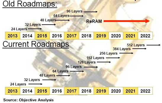
The other interesting thing that Handy showed was that how the 3D NAND and other persistent storage roadmaps, which expected for the commercialization of resistive RAM (ReRAM) to start ramping sometime around next year, have been torn up as 3D NAND makers have figured out ways to add more and more layers of cells in their flash and therefore extended the technical and economic life of flash memory.
While flash has found itself a home as an accelerator for DRAM as well as a replacement for disk drives in certain applications, Handy is also optimistic about the 3D XPoint memory developed together by Intel and Micron Technology and which they are selling separately. The Optane SSDs, in both traditional disk enclosure and M.2 and U.2 gum stick form factors, as shipping in PCs, but everyone, including Handy and us, expect for the Optane DIMM form factors to be the natural choice for expanding main memory footprints and lowering the overall cost per GB for that main memory. We don’t know what the price and performance of 3D XPoint will be for these DIMMs, but what we do know is that 3D XPoint will be faster than NAND flash but slower than DDR4 main memory and will be costlier than NAND flash but cheaper than DRAM. The “Purley” platform that will support the current “Skylake” Xeon SP processors and the future “Cascade Lake” chips from Intel was designed from the get-go to support Intel’s “Apache Pass” Optane memory sticks and will eventually have BIOS and firmware support added to them so they can be addressed as either slow main memory or very fast persistent storage. The persistence is the hard bit, since DDR memory controllers can already support main memory running at different speeds. Handy notes that Linux has started up its pmem.io initiative to add persistent memory to the hierarchy. Windows Server got its initial patches for persistent memory last fall, with NVDIMM support, and Optane DIMMs will no doubt build on this. The Storage Networking Industry Association that develops standards in this area is developing a persistent memory programming standard to help push the efforts along.
The issue as far as Handy can see if that 3D XPoint has the classis egg-chicken problem: 3D XPoint has to cost less than DRAM to ship in volume, but it won’t ship in volume until the price drops below DRAM. So in our analysis, we are counting on scenarios where 3D XPoint will be used in PCs and servers in SSD form factors as accelerators between flash and DDR4 memory to drive down the price of 3D XPoint chips to the point where Intel can maker cheaper 3D XPoint DIMMs. This will probably happen, all luck being what it is, about the time that the 3D NAND crash comes in late 2018 or early 2019, which will make it even harder to sell 3D XPoint because prices will plummet for flash. If Intel and Micron try to shift capacity from flash to 3D XPoint, other flash vendors will massively undercut them and hurt their revenue streams for flash. So they are not going to let them happen. They are going to ride the process curves, do as much volume on all of the memory fronts that they can, and hope for the best.
Five years ago, Marks explained in his presentation, flash was still a point solution in the enterprise, and before that it was an exotic solution where very high I/O operations per second were justified – Facebook’s and Apple’s underpinnings of their vast MySQL databases with flash to speed up database access is the killer app for flash, and we think Google was probably ahead of them with flash acceleration on Google File System, Colossus, BigTable, and other file systems and data stores at the search engine and ad serving giant. Now, in the enterprise, the 3D TLC NAND flash has become standard, and flash devices rival or beat the capacities of enterprise-grade SAS and SATA disks. The largest 3D NAND flash devices using the PCI-Express peripheral bus cram 64 TB in an add-in card, 7.6 TB in a U.2 drive form factor, and 8 TB in an M.2 memory stick. SAS drives top out at 15.8 TB and SATA drives around 4 TB, so in terms of the capacity battle, flash has won.
Marks called out the UHC-Silo 50 TB SSD from Viking Technology for long-term, relatively cold storage for hyperscalers and very large enterprises wanting to ditch disks, but this 3.5-inch SSD only supports 6 Gb/sec ports and one drive write per day at its 350 MB/sec sequential write bandwidth. The drive is rated at 60,000 IOPS for random reads and 15,000 IOPS for random writes, and can manage only 500 MB/sec on sequential reads. As such, this Viking unit is really only for the long tail. Which the flash industry needs if flash is to replace disk.
Show And Tell
As a theoretical shopper of system components for the next platforms of the world, a couple of different flash devices caught our eyes at the Flash Memory Summit and we thought we would bring them to your attention.
This time last year, Seagate Technology was showing off a super-fat 60 TB flash SSD in a 3.5-inch form factor. This year, Seagate has tweaked it a little to get it out of a niche, cold storage use case. In last year’s model this drive was in a SAS SSD form factor and topped out at 12 Gb/sec connectivity, Kent Smith, senior director of product marketing at Seagate, tells The Next Platform. So Seagate went back to the drawing board and grabbed the hot off the etchers 512 Gb 3D TLC NAND chips from Micron (and will be able to move to QLC chips when they are available), added an NVM-Express controller, and put it on a PCI-Express x16 card slot to create a full height, half length flash card that weighs in at 64 TB. Here are the feeds and speeds:
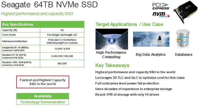
This particular unit is being subbed as the fattest and fastest SSD card in the world, and 2 million IOPS on random reads all by its lonesome. This as-yet-unnamed flash card has eight flash controllers that are linked to the PCI-Express bus by a PCI-Express switch on the card, and it is partitioned as eight separate flash volumes. The point is, by creating what is in essence a storage cluster on a card, Seagate can saturate the PCI-Express bus on reads.
As for pricing on this beast, Smith says it has not been set yet, but says that for client and consumer flash devices, the prices range from around 25 cents to 33 cents per GB, and that for typical enterprise stuff you are looking at maybe 50 cents to 75 cents per GB, with a top-end of $3 per GB for the really extreme stuff. So don’t expect this fat and fast flash card to be cheap when it starts shipping after Micron rolls out the 512 Gb 3D TLC flash chips early next year for production. The neat thing is that a JBOF enclosure with sixteen of these would reach 1 PB of aggregate raw capacity.
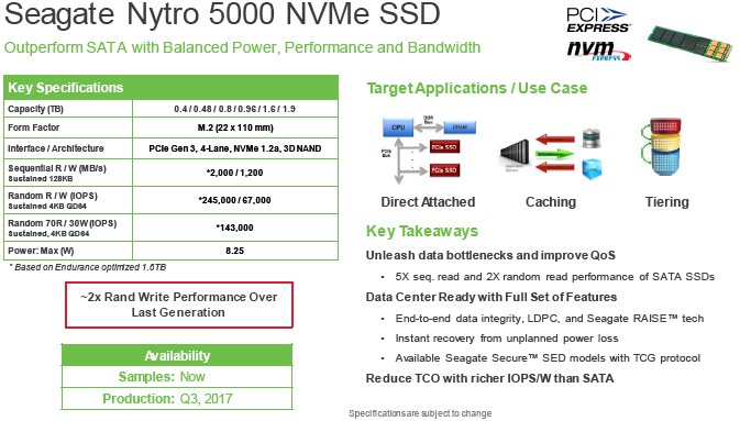
Seagate also rolled out the Nytro 5000 M.2 SSD, which also supports NVM-Express, its third generation of these M.2 devices. For this generation, Smith says that Seagate focused on boosting random write performance, which is twice that of the earlier 1440 series. It is hard to push performance any higher because this Nytro 5000 is saturating the M.2 bus, which hits a ceiling at 2 GB/sec.
For its more mainstream capacity flash, Seagate also rolled out the sixth generation of its 2.5-inch SAS enterprise drives, and the Nytro 3000 will be the first devices that can put 15 TB into this form factor using that protocol from Seagate. Here are the feeds and speeds:
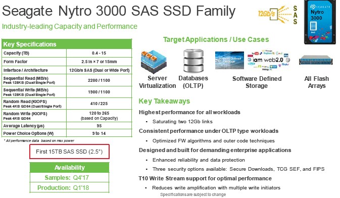
Smith puts a stake in the ground and says Seagate expects the Nytro 3000 to be the fastest 15 TB drive on the market. Production begins in the first quarter of 2018.
Perhaps the most interesting thing that Seagate did at Flash Memory Summit was not rolling out new hardware, but a special set of acceleration software for its flash devices that it is developing in conjunction with hyperscalers Microsoft and Facebook called Nytro Q-Boost. This software, which will be packaged separately from the controllers, possibly with a 10 percent to 20 percent premium on the flash device cost, helps with providing consistent and lower latencies on reads and writes on systems with mixed workloads and also helps cut down on write amplification, which is bad for flash.
The first issue deals with I/O determinism, and a simple scenario explains it. Say you have a server with two applications on it, and they are sharing a flash device. Under normal operation, the server and the flash have no idea when App A is writing to the drive at the same time as App B is reading to it, but the controller can do both at the same time – and vice versa on the reads and writes. This can cause a huge conflict in read latencies for an application. But with the I/O determinism feature of Nytro Q-Boost, which is aware of reading and writing by distinct applications, the read latencies can be made more predictable and significantly lowered – by a factor of 16X in the performance test shown below:
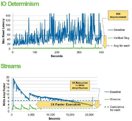
In this test above, the average read latency of applications is around 55 milliseconds, and that is quite frankly not that good considering the speed of flash devices today. But after Q-Boost was installed and the queuing and quality of service software was set up on the flash, the average read latency dropped to a pretty flat 3.5 milliseconds. The way it works is that the data for particular applications are put onto specific flash dies on the device, and the Q-Boost keeps track of these and allows parallel and concurrent access to different regions of flash and their semi-dedicated flash segments, without any conflicts. The applications still share a controller, but it is virtualized, spreading out reads and writes concurrently without conflicts. Q-Boost is an enterprise feature, and should work on any Seagate drive. It is being tested in the labs now, and could be available early next year or later this year.
The multi-streams feature of Q-Boost is a means of better placing data on the flash capacity to make it possible to reduce garbage collection and the ensuing write amplification that is common to all flash memory. Flash writes in pages, but it erases data in whole blocks, and so when you want to overwrite data with updated data, you have to find all of pages that have valid information and move them to a new block and then erase the old blocks so they can receive new data; the host server only writes the data once, but the flash controller has to keep moving it around, writing it again and again as it is reassembled in its new form. This is bad because flash cells have a limited number of writes before they fizzle. The idea with multi-streams is to keep data that is changing away from data that is not changing on the blocks in the flash capacity – that way, you are not moving around so many blocks and erasing them as a portion of the data changes.
In the performance data above, the distribution of write amplifications goes from a high of around twenty times to a baseline average of around six times. With the multi-streams feature, the execution of the writes is about 3X faster, and the number of writes averages around two times with a peak of around four times – a factor of 3X to 5X improvement there.
One Ruler To Rule Them All
Over at Intel, the company did a lot of talking about how early adopters were deploying its Optane 3D XPoint SSDs, consistent with the message we have been seeing for months, and mentioned its new flash devices as almost an afterthought. The company also debuted a new form factor it is calling “ruler” that is one big, long SSD that is intended to slide into the fill length of a server chassis and also allow for up to 1 PB of flash storage in a 1U server enclosure.
The new DC S4500 and DC S4600 flash drives come in 2.5-inch form factors and are only 7 millimeters high, and sport the second generation of 32-layer 3D TLC NAND chips from Intel. Rather than go for big fat devices, Intel is working on skinny ones. The DC S4500s have a single 6 Gb/sec SATA port and range in capacity from 240 GB to 3.84 TB. The DC S4600s have the same basic feeds and speeds, but burn a little less juice and have a much higher endurance (three drive writes per day instead of one). Intel has also rolled out dual-port Optane SSDs, which will come in handy in the datacenter.
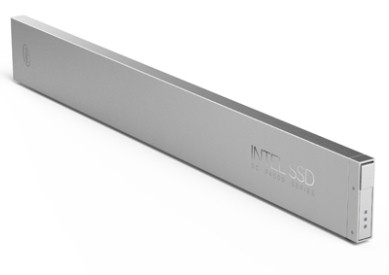
The neatest thing from Intel was the ruler form factor, which will be stuffed with NAND flash and 3D XPoint memory and pack more memory into skinny or fat servers than can be done with other form factors. Here is what the ruler form factor looks like:
And here is what it looks like in a 1U server jammed with a bunch of them:
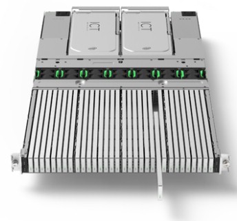
With the ruler form factor, Intel can get 32 rulers of flash or 3D XPoint into a 1U server, and in 2018 the company says that will mean more than 1 PB of capacity of then-shipping 3D NAND flash. By way of comparison, using 2 TB disk drives, it used to take a whole rack of 21 storage servers to reach 1 PB a few years back before flash got dense. This is how Intel sees the rule form factor stacking up to those available on the market from many different suppliers:
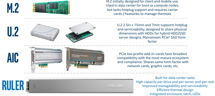
While the U.2 form factor keeps the same dimensions of the disk drive and the M.2 gum stick card has a much smaller form factor that is good for some uses in the datacenter, such as for boot devices and scratch pads, neither are optimized for density or low cost, and the M.2 stick has limited capacity. The ruler form factor can have six times as many flash chips (it measures 325.34 mm by 38.6 mm). If you compare that to 15 mm U.2 devices, a 2U server with 24 of these devices, each weighing in at the typical 4 TB capacity yields a total of 48 TB per server. With the ruler SSD, each ruler weighs in at 8 TB and with 32 of them, a 1U server can do 256 TB, and two of them could do 512 TB, for more than an order of magnitude better flash density in the system.
At the right price, and performance, this could be quite compelling, and help drive more flash into datacenters. And, it also looks cool and modern and modular.
We will be covering other things we learned from Flash Memory Summit. Stay tuned.

Taking A Deep Dive Into “Cooper Lake” Xeon SP Processors
Even before the coronavirus pandemic hit, Intel, the dominant maker of processors for servers on the planet, was rejiggering its product roadmaps behind the scenes in conjunction with its largest OEM partners as well the hyperscalers and large public cloud builders that drive about a third of its revenues these …

Finally, The Right Pilot At The Intel Helm
Running a company of any size is the hardest thing you will ever do. And having run a few of them ourselves here at The Next Platform, when we see companies in the IT sector struggling and executives trying to steer their companies between Scylla and Charybdis, our first reaction …
The Datacenter GPU Gravy Train That No One Will Derail
We have five decades of very fine-grained analysis of CPU compute engines in the datacenter, and changes come at a steady but glacial pace when it comes to CPU serving. The rise of datacenter GPU compute engines has happened in a very short decade and a half, and yet there …
Intel is again claiming any innovative idea but in reality it is only thanks to ignorance of peoples, which don’t realize, that it is already few years on market.
The ruler form factor is impressive, and I am sure it will be many years before we see it on a storage array. While it is dense, isn’t it eating away space which is needed for compute? May be the nodes that will use ruler form factor SSDs will be dense in storage and less in compute capacity.
I would also like to call out Dell EMC DSSD, which had something like this. I mean, in DSSD they didn’t use 2.5″ or 3.5″ form factor SSD instead they created flash modules which looked very very similar to the ruler form factor that Intel has introduced. The flash modules in DSSD were slim like the ruler SSD, but they were taller and shorter.